- 您现在的位置:买卖IC网 > PDF目录11406 > PIC18F2510-E/ML (Microchip Technology)IC PIC MCU FLASH 16KX16 28QFN PDF资料下载
参数资料
| 型号: | PIC18F2510-E/ML |
| 厂商: | Microchip Technology |
| 文件页数: | 206/234页 |
| 文件大小: | 0K |
| 描述: | IC PIC MCU FLASH 16KX16 28QFN |
| 产品培训模块: | Asynchronous Stimulus PIC18 J Series MCU Overview |
| 标准包装: | 61 |
| 系列: | PIC® 18F |
| 核心处理器: | PIC |
| 芯体尺寸: | 8-位 |
| 速度: | 25MHz |
| 连通性: | I²C,SPI,UART/USART |
| 外围设备: | 欠压检测/复位,HLVD,POR,PWM,WDT |
| 输入/输出数: | 25 |
| 程序存储器容量: | 32KB(16K x 16) |
| 程序存储器类型: | 闪存 |
| RAM 容量: | 1.5K x 8 |
| 电压 - 电源 (Vcc/Vdd): | 4.2 V ~ 5.5 V |
| 数据转换器: | A/D 10x10b |
| 振荡器型: | 内部 |
| 工作温度: | -40°C ~ 125°C |
| 封装/外壳: | 28-VQFN 裸露焊盘 |
| 包装: | 管件 |
第1页第2页第3页第4页第5页第6页第7页第8页第9页第10页第11页第12页第13页第14页第15页第16页第17页第18页第19页第20页第21页第22页第23页第24页第25页第26页第27页第28页第29页第30页第31页第32页第33页第34页第35页第36页第37页第38页第39页第40页第41页第42页第43页第44页第45页第46页第47页第48页第49页第50页第51页第52页第53页第54页第55页第56页第57页第58页第59页第60页第61页第62页第63页第64页第65页第66页第67页第68页第69页第70页第71页第72页第73页第74页第75页第76页第77页第78页第79页第80页第81页第82页第83页第84页第85页第86页第87页第88页第89页第90页第91页第92页第93页第94页第95页第96页第97页第98页第99页第100页第101页第102页第103页第104页第105页第106页第107页第108页第109页第110页第111页第112页第113页第114页第115页第116页第117页第118页第119页第120页第121页第122页第123页第124页第125页第126页第127页第128页第129页第130页第131页第132页第133页第134页第135页第136页第137页第138页第139页第140页第141页第142页第143页第144页第145页第146页第147页第148页第149页第150页第151页第152页第153页第154页第155页第156页第157页第158页第159页第160页第161页第162页第163页第164页第165页第166页第167页第168页第169页第170页第171页第172页第173页第174页第175页第176页第177页第178页第179页第180页第181页第182页第183页第184页第185页第186页第187页第188页第189页第190页第191页第192页第193页第194页第195页第196页第197页第198页第199页第200页第201页第202页第203页第204页第205页当前第206页第207页第208页第209页第210页第211页第212页第213页第214页第215页第216页第217页第218页第219页第220页第221页第222页第223页第224页第225页第226页第227页第228页第229页第230页第231页第232页第233页第234页
2009 Microchip Technology Inc.
DS39636D-page 75
PIC18F2X1X/4X1X
5.5.3
MAPPING THE ACCESS BANK IN
INDEXED LITERAL OFFSET
ADDRESSING MODE
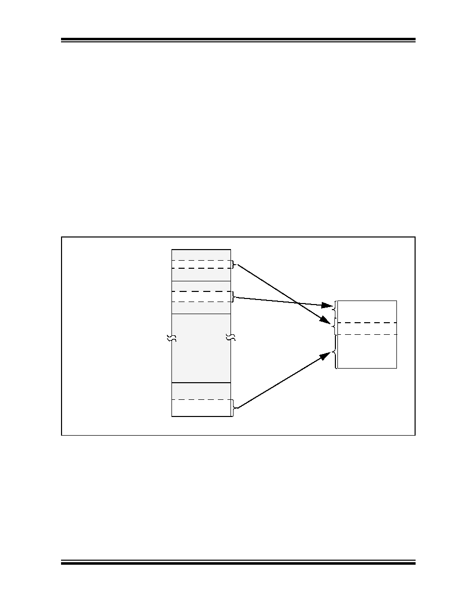
The use of Indexed Literal Offset Addressing mode
effectively changes how the first 96 locations of access
RAM (00h to 5Fh) are mapped. Rather than containing
just the contents of the bottom half of Bank 0, this mode
maps the contents from Bank 0 and a user defined
“window” that can be located anywhere in the data
memory space. The value of FSR2 establishes the
lower boundary of the addresses mapped into the
window, while the upper boundary is defined by FSR2
plus 95 (5Fh). Addresses in the Access RAM above
5Fh are mapped as previously described (see
Section 5.3.2 “Access Bank”). An example of Access
Bank remapping in this addressing mode is shown in
Remapping of the Access Bank applies only to opera-
tions using the Indexed Literal Offset Addressing
mode. Operations that use the BSR (Access RAM bit is
‘1’) will continue to use direct addressing as before.
5.6
PIC18 Instruction Execution and
the Extended Instruction Set
Enabling the extended instruction set adds eight
additional commands to the existing PIC18 instruction
set. These instructions are executed as described in
FIGURE 5-11:
REMAPPING THE ACCESS BANK WITH INDEXED LITERAL OFFSET
ADDRESSING
Data Memory
000h
100h
200h
F80h
F00h
FFFh
Bank 1
Bank 15
Bank 2
through
Bank 14
SFRs
05Fh
ADDWF f, d, a
FSR2H:FSR2L = 120h
Locations in the region
from the FSR2 Pointer
(120h) to the pointer plus
05Fh (17Fh) are mapped
to the bottom of the
Access RAM (000h-05Fh).
Locations in Bank 0 from
060h to 07Fh are mapped,
as usual, to the middle of
the Access Bank.
Special File Registers at
F80h through FFFh are
mapped to 80h through
FFh, as usual.
Bank 0 addresses below
5Fh can still be addressed
by using the BSR.
Access Bank
00h
80h
FFh
7Fh
Bank 0
SFRs
Bank 1 “Window”
Bank 0
Bank 0
Window
Example Situation:
07Fh
120h
17Fh
5Fh
Bank 1
相关PDF资料 |
PDF描述 |
|---|---|
| VE-2NB-CV-F4 | CONVERTER MOD DC/DC 95V 150W |
| DSPIC30F3011-30I/ML | IC DSPIC MCU/DSP 24K 44QFN |
| VE-2NB-CV-F3 | CONVERTER MOD DC/DC 95V 150W |
| PIC16C56-LPE/SO | IC MCU OTP 1KX12 18SOIC |
| PIC16C558-20I/SO | IC MCU OTP 2KX14 18SOIC |
相关代理商/技术参数 |
参数描述 |
|---|---|
| PIC18F2510-I/ML | 功能描述:8位微控制器 -MCU 32kBF 1536RM 25I/O RoHS:否 制造商:Silicon Labs 核心:8051 处理器系列:C8051F39x 数据总线宽度:8 bit 最大时钟频率:50 MHz 程序存储器大小:16 KB 数据 RAM 大小:1 KB 片上 ADC:Yes 工作电源电压:1.8 V to 3.6 V 工作温度范围:- 40 C to + 105 C 封装 / 箱体:QFN-20 安装风格:SMD/SMT |
| PIC18F2510-I/SO | 功能描述:8位微控制器 -MCU 32KB 1536 RAM 25I/O RoHS:否 制造商:Silicon Labs 核心:8051 处理器系列:C8051F39x 数据总线宽度:8 bit 最大时钟频率:50 MHz 程序存储器大小:16 KB 数据 RAM 大小:1 KB 片上 ADC:Yes 工作电源电压:1.8 V to 3.6 V 工作温度范围:- 40 C to + 105 C 封装 / 箱体:QFN-20 安装风格:SMD/SMT |
| PIC18F2510-I/SP | 功能描述:8位微控制器 -MCU 32KB 1536 RAM 25I/O RoHS:否 制造商:Silicon Labs 核心:8051 处理器系列:C8051F39x 数据总线宽度:8 bit 最大时钟频率:50 MHz 程序存储器大小:16 KB 数据 RAM 大小:1 KB 片上 ADC:Yes 工作电源电压:1.8 V to 3.6 V 工作温度范围:- 40 C to + 105 C 封装 / 箱体:QFN-20 安装风格:SMD/SMT |
| PIC18F2510T-I/ML | 功能描述:8位微控制器 -MCU 32KB 1536 RAM 25I/O RoHS:否 制造商:Silicon Labs 核心:8051 处理器系列:C8051F39x 数据总线宽度:8 bit 最大时钟频率:50 MHz 程序存储器大小:16 KB 数据 RAM 大小:1 KB 片上 ADC:Yes 工作电源电压:1.8 V to 3.6 V 工作温度范围:- 40 C to + 105 C 封装 / 箱体:QFN-20 安装风格:SMD/SMT |
| PIC18F2510T-I/SO | 功能描述:8位微控制器 -MCU 32KB 1536 RAM 25I/O RoHS:否 制造商:Silicon Labs 核心:8051 处理器系列:C8051F39x 数据总线宽度:8 bit 最大时钟频率:50 MHz 程序存储器大小:16 KB 数据 RAM 大小:1 KB 片上 ADC:Yes 工作电源电压:1.8 V to 3.6 V 工作温度范围:- 40 C to + 105 C 封装 / 箱体:QFN-20 安装风格:SMD/SMT |
发布紧急采购,3分钟左右您将得到回复。