- 您现在的位置:买卖IC网 > PDF目录11502 > PIC18F25J10-I/ML (Microchip Technology)IC PIC MCU FLASH 16KX16 28QFN PDF资料下载
参数资料
| 型号: | PIC18F25J10-I/ML |
| 厂商: | Microchip Technology |
| 文件页数: | 51/80页 |
| 文件大小: | 0K |
| 描述: | IC PIC MCU FLASH 16KX16 28QFN |
| 产品培训模块: | Asynchronous Stimulus PIC18 J Series MCU Overview 8-bit PIC® Microcontroller Portfolio |
| 标准包装: | 61 |
| 系列: | PIC® 18F |
| 核心处理器: | PIC |
| 芯体尺寸: | 8-位 |
| 速度: | 40MHz |
| 连通性: | I²C,SPI,UART/USART |
| 外围设备: | 欠压检测/复位,POR,PWM,WDT |
| 输入/输出数: | 21 |
| 程序存储器容量: | 32KB(16K x 16) |
| 程序存储器类型: | 闪存 |
| RAM 容量: | 1K x 8 |
| 电压 - 电源 (Vcc/Vdd): | 2.7 V ~ 3.6 V |
| 数据转换器: | A/D 10x10b |
| 振荡器型: | 内部 |
| 工作温度: | -40°C ~ 85°C |
| 封装/外壳: | 28-VQFN 裸露焊盘 |
| 包装: | 管件 |
| 产品目录页面: | 643 (CN2011-ZH PDF) |
| 配用: | AC162074-ND - HEADER INTRFC MPLAB ICD2 44TQFP MA180011-ND - MODULE PLUG-IN 18F25J10 28SOIC AC162067-ND - HEADER INTRFC MPLAB ICD2 40/28P |
第1页第2页第3页第4页第5页第6页第7页第8页第9页第10页第11页第12页第13页第14页第15页第16页第17页第18页第19页第20页第21页第22页第23页第24页第25页第26页第27页第28页第29页第30页第31页第32页第33页第34页第35页第36页第37页第38页第39页第40页第41页第42页第43页第44页第45页第46页第47页第48页第49页第50页当前第51页第52页第53页第54页第55页第56页第57页第58页第59页第60页第61页第62页第63页第64页第65页第66页第67页第68页第69页第70页第71页第72页第73页第74页第75页第76页第77页第78页第79页第80页
PIC16F8X
1998 Microchip Technology Inc.
DS30430C-page 55
9.0
INSTRUCTION SET SUMMARY
Each PIC16CXX instruction is a 14-bit word divided
into an OPCODE which specifies the instruction type
and one or more operands which further specify the
operation of the instruction. The PIC16CXX instruction
set summary in Table 9-2 lists byte-oriented, bit-ori-
ented, and literal and control operations. Table 9-1
shows the opcode field descriptions.
For byte-oriented instructions, ’f’ represents a file reg-
ister designator and ’d’ represents a destination desig-
nator. The file register designator specifies which file
register is to be used by the instruction.
The destination designator specifies where the result of
the operation is to be placed. If ’d’ is zero, the result is
placed in the W register. If ’d’ is one, the result is placed
in the file register specified in the instruction.
For bit-oriented instructions, ’b’ represents a bit field
designator which selects the number of the bit affected
by the operation, while ’f’ represents the number of the
file in which the bit is located.
For literal and control operations, ’k’ represents an
eight or eleven bit constant or literal value.
TABLE 9-1
OPCODE FIELD
DESCRIPTIONS
The instruction set is highly orthogonal and is grouped
into three basic categories:
Byte-oriented operations
Bit-oriented operations
Literal and control operations
All instructions are executed within one single instruc-
tion cycle, unless a conditional test is true or the pro-
gram counter is changed as a result of an instruction.
In this case, the execution takes two instruction cycles
with the second cycle executed as a NOP. One instruc-
tion cycle consists of four oscillator periods. Thus, for
an oscillator frequency of 4 MHz, the normal instruction
execution time is 1
s. If a conditional test is true or the
program counter is changed as a result of an instruc-
tion, the instruction execution time is 2
s.
Table 9-2 lists the instructions recognized by the
MPASM assembler.
Figure 9-1 shows the general formats that the instruc-
tions can have.
All examples use the following format to represent a
hexadecimal number:
0xhh
where h signifies a hexadecimal digit.
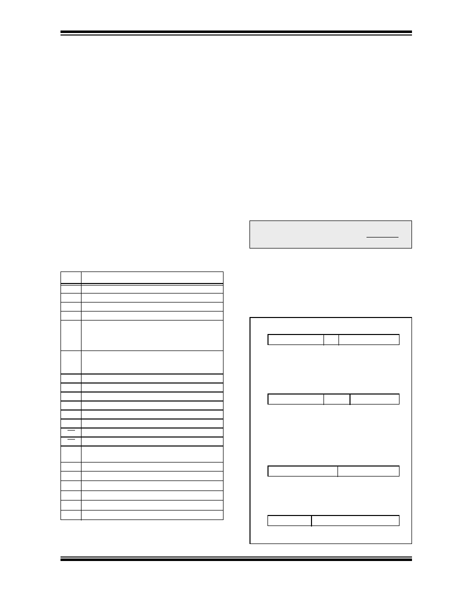
FIGURE 9-1:
GENERAL FORMAT FOR
INSTRUCTIONS
Field
Description
f
Register file address (0x00 to 0x7F)
W
Working register (accumulator)
b
Bit address within an 8-bit file register
k
Literal field, constant data or label
x
Don’t care location (= 0 or 1)
The assembler will generate code with x = 0. It is the
recommended form of use for compatibility with all
Microchip software tools.
d
Destination select; d = 0: store result in W,
d = 1: store result in file register f.
Default is d = 1
label
Label name
TOS
Top of Stack
PC
Program Counter
PCLATH
Program Counter High Latch
GIE
Global Interrupt Enable bit
WDT
Watchdog Timer/Counter
TO
Time-out bit
PD
Power-down bit
dest
Destination either the W register or the specified
register file location
[ ]
Options
( )
Contents
→
Assigned to
< >
Register bit field
∈
In the set of
italics
User defined term (font is courier)
Note:
To maintain upward compatibility with
future PIC16CXX products, do not use the
OPTION
and TRIS instructions.
Byte-oriented file register operations
13
8
7
6
0
d = 0 for destination W
OPCODE
d
f (FILE #)
d = 1 for destination f
f = 7-bit file register address
Bit-oriented file register operations
13
10 9
7 6
0
OPCODE
b (BIT #)
f (FILE #)
b = 3-bit bit address
f = 7-bit file register address
Literal and control operations
13
8
7
0
OPCODE
k (literal)
k = 8-bit immediate value
13
11
10
0
OPCODE
k (literal)
k = 11-bit immediate value
General
CALL
and GOTO instructions only
相关PDF资料 |
PDF描述 |
|---|---|
| PIC16LF819T-I/ML | IC MCU FLASH 2KX14 EEPROM 28QFN |
| VE-B0D-IY-B1 | CONVERTER MOD DC/DC 85V 50W |
| PIC16LC770-I/SO | IC MCU OTP 2KX14 A/D PWM 20SOIC |
| PIC16C710-20I/SO | IC MCU OTP 512X14 A/D 18SOIC |
| VE-B0B-IY-B1 | CONVERTER MOD DC/DC 95V 50W |
相关代理商/技术参数 |
参数描述 |
|---|---|
| PIC18F25J10T-I/ML | 功能描述:8位微控制器 -MCU 32 KB FL 1024 RAM RoHS:否 制造商:Silicon Labs 核心:8051 处理器系列:C8051F39x 数据总线宽度:8 bit 最大时钟频率:50 MHz 程序存储器大小:16 KB 数据 RAM 大小:1 KB 片上 ADC:Yes 工作电源电压:1.8 V to 3.6 V 工作温度范围:- 40 C to + 105 C 封装 / 箱体:QFN-20 安装风格:SMD/SMT |
| PIC18F25J10T-I/SO | 功能描述:8位微控制器 -MCU 32 KB FL 1024 RAM RoHS:否 制造商:Silicon Labs 核心:8051 处理器系列:C8051F39x 数据总线宽度:8 bit 最大时钟频率:50 MHz 程序存储器大小:16 KB 数据 RAM 大小:1 KB 片上 ADC:Yes 工作电源电压:1.8 V to 3.6 V 工作温度范围:- 40 C to + 105 C 封装 / 箱体:QFN-20 安装风格:SMD/SMT |
| PIC18F25J10T-I/SS | 功能描述:8位微控制器 -MCU 16 KB FL 1 KB RAM RoHS:否 制造商:Silicon Labs 核心:8051 处理器系列:C8051F39x 数据总线宽度:8 bit 最大时钟频率:50 MHz 程序存储器大小:16 KB 数据 RAM 大小:1 KB 片上 ADC:Yes 工作电源电压:1.8 V to 3.6 V 工作温度范围:- 40 C to + 105 C 封装 / 箱体:QFN-20 安装风格:SMD/SMT |
| PIC18F25J11-I/ML | 功能描述:8位微控制器 -MCU 32KB Flash 4KBRAM 12MIPS nanoWatt RoHS:否 制造商:Silicon Labs 核心:8051 处理器系列:C8051F39x 数据总线宽度:8 bit 最大时钟频率:50 MHz 程序存储器大小:16 KB 数据 RAM 大小:1 KB 片上 ADC:Yes 工作电源电压:1.8 V to 3.6 V 工作温度范围:- 40 C to + 105 C 封装 / 箱体:QFN-20 安装风格:SMD/SMT |
| PIC18F25J11-I/SO | 功能描述:8位微控制器 -MCU 32KB Flash 4KBRAM 12MIPS nanoWatt RoHS:否 制造商:Silicon Labs 核心:8051 处理器系列:C8051F39x 数据总线宽度:8 bit 最大时钟频率:50 MHz 程序存储器大小:16 KB 数据 RAM 大小:1 KB 片上 ADC:Yes 工作电源电压:1.8 V to 3.6 V 工作温度范围:- 40 C to + 105 C 封装 / 箱体:QFN-20 安装风格:SMD/SMT |
发布紧急采购,3分钟左右您将得到回复。