- 您现在的位置:买卖IC网 > PDF目录11377 > PIC18F2610-I/SO (Microchip Technology)IC MCU FLASH 32KX16 28SOIC PDF资料下载
参数资料
| 型号: | PIC18F2610-I/SO |
| 厂商: | Microchip Technology |
| 文件页数: | 230/234页 |
| 文件大小: | 0K |
| 描述: | IC MCU FLASH 32KX16 28SOIC |
| 产品培训模块: | Asynchronous Stimulus 8-bit PIC® Microcontroller Portfolio |
| 标准包装: | 27 |
| 系列: | PIC® 18F |
| 核心处理器: | PIC |
| 芯体尺寸: | 8-位 |
| 速度: | 40MHz |
| 连通性: | I²C,SPI,UART/USART |
| 外围设备: | 欠压检测/复位,HLVD,POR,PWM,WDT |
| 输入/输出数: | 25 |
| 程序存储器容量: | 64KB(32K x 16) |
| 程序存储器类型: | 闪存 |
| RAM 容量: | 3.8K x 8 |
| 电压 - 电源 (Vcc/Vdd): | 4.2 V ~ 5.5 V |
| 数据转换器: | A/D 10x10b |
| 振荡器型: | 内部 |
| 工作温度: | -40°C ~ 85°C |
| 封装/外壳: | 28-SOIC(0.295",7.50mm 宽) |
| 包装: | 管件 |
| 产品目录页面: | 644 (CN2011-ZH PDF) |
| 配用: | XLT28SO-1-ND - SOCKET TRANSITION 28SOIC 300MIL |
第1页第2页第3页第4页第5页第6页第7页第8页第9页第10页第11页第12页第13页第14页第15页第16页第17页第18页第19页第20页第21页第22页第23页第24页第25页第26页第27页第28页第29页第30页第31页第32页第33页第34页第35页第36页第37页第38页第39页第40页第41页第42页第43页第44页第45页第46页第47页第48页第49页第50页第51页第52页第53页第54页第55页第56页第57页第58页第59页第60页第61页第62页第63页第64页第65页第66页第67页第68页第69页第70页第71页第72页第73页第74页第75页第76页第77页第78页第79页第80页第81页第82页第83页第84页第85页第86页第87页第88页第89页第90页第91页第92页第93页第94页第95页第96页第97页第98页第99页第100页第101页第102页第103页第104页第105页第106页第107页第108页第109页第110页第111页第112页第113页第114页第115页第116页第117页第118页第119页第120页第121页第122页第123页第124页第125页第126页第127页第128页第129页第130页第131页第132页第133页第134页第135页第136页第137页第138页第139页第140页第141页第142页第143页第144页第145页第146页第147页第148页第149页第150页第151页第152页第153页第154页第155页第156页第157页第158页第159页第160页第161页第162页第163页第164页第165页第166页第167页第168页第169页第170页第171页第172页第173页第174页第175页第176页第177页第178页第179页第180页第181页第182页第183页第184页第185页第186页第187页第188页第189页第190页第191页第192页第193页第194页第195页第196页第197页第198页第199页第200页第201页第202页第203页第204页第205页第206页第207页第208页第209页第210页第211页第212页第213页第214页第215页第216页第217页第218页第219页第220页第221页第222页第223页第224页第225页第226页第227页第228页第229页当前第230页第231页第232页第233页第234页
2009 Microchip Technology Inc.
DS39636D-page 97
PIC18F2X1X/4X1X
9.0
I/O PORTS
Depending on the device selected and features
enabled, there are up to five ports available. Some pins
of the I/O ports are multiplexed with an alternate
function from the peripheral features on the device. In
general, when a peripheral is enabled, that pin may not
be used as a general purpose I/O pin.
Each port has three registers for its operation. These
registers are:
TRIS register (data direction register)
PORT register (reads the levels on the pins of the
device)
LAT register (output latch)
The Data Latch (LAT register) is useful for read-modify-
write operations on the value that the I/O pins are
driving.
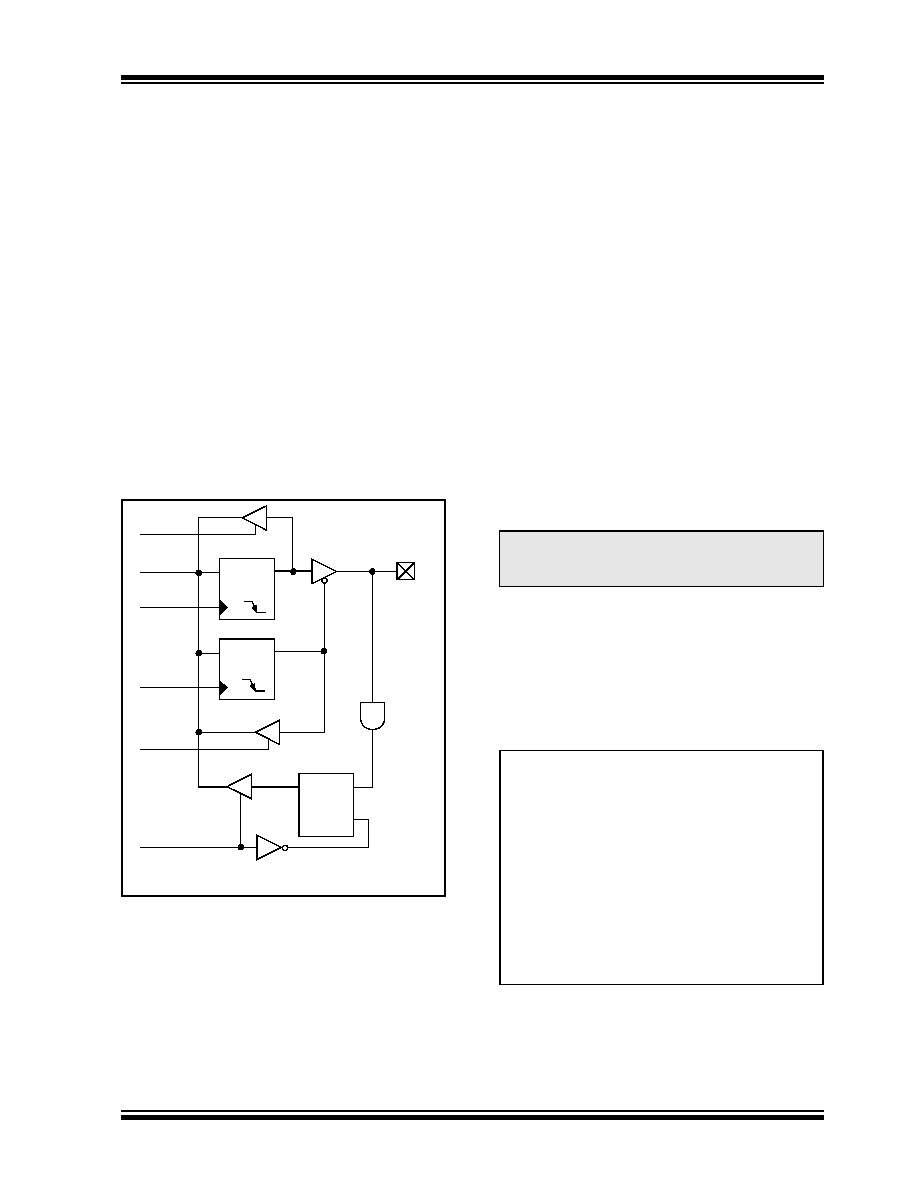
A simplified model of a generic I/O port, without the
interfaces to other peripherals, is shown in Figure 9-1.
FIGURE 9-1:
GENERIC I/O PORT
OPERATION
9.1
PORTA, TRISA and LATA Registers
PORTA is a 8-bit wide, bidirectional port. The corre-
sponding data direction register is TRISA. Setting a
TRISA bit (= 1) will make the corresponding PORTA pin
an input (i.e., put the corresponding output driver in a
high-impedance mode). Clearing a TRISA bit (= 0) will
make the corresponding PORTA pin an output (i.e., put
the contents of the output latch on the selected pin).
Reading the PORTA register reads the status of the
pins, whereas writing to it will write to the port latch.
The Data Latch (LATA) register is also memory mapped.
Read-modify-write operations on the LATA register read
and write the latched output value for PORTA.
The RA4 pin is multiplexed with the Timer0 module
clock input and one of the comparator outputs to
become the RA4/T0CKI/C1OUT pin. Pins RA6 and
RA7 are multiplexed with the main oscillator pins; they
are enabled as oscillator or I/O pins by the selection of
the main oscillator in the Configuration register (see
Section 22.1 “Configuration Bits” for details). When
they are not used as port pins, RA6 and RA7 and their
associated TRIS and LAT bits are read as ‘0’.
The other PORTA pins are multiplexed with analog
inputs, the analog VREF+ and VREF- inputs and the com-
parator voltage reference output. The operation of pins
RA3:RA0 and RA5 as A/D converter inputs is selected
by clearing or setting the control bits in the ADCON1
register (A/D Control Register 1).
Pins RA0 through RA5 may also be used as comparator
inputs or outputs by setting the appropriate bits in the
CMCON register. To use RA3:RA0 as digital inputs, it is
also necessary to turn off the comparators.
The RA4/T0CKI/C1OUT pin is a Schmitt Trigger input.
All other PORTA pins have TTL input levels and full
CMOS output drivers.
The TRISA register controls the direction of the PORTA
pins, even when they are being used as analog inputs.
The user must ensure the bits in the TRISA register are
maintained set when using them as analog inputs.
EXAMPLE 9-1:
INITIALIZING PORTA
Data
Bus
WR LAT
WR TRIS
RD Port
Data Latch
TRIS Latch
RD TRIS
Input
Buffer
I/O pin(1)
Q
D
CK
Q
D
CK
EN
QD
EN
RD LAT
or Port
Note 1:
I/O pins have diode protection to VDD and VSS.
Note:
On a Power-on Reset, RA5 and RA3:RA0
are configured as analog inputs and read
as ‘0’. RA4 is configured as a digital input.
CLRF
PORTA
; Initialize PORTA by
; clearing output
; data latches
CLRF
LATA
; Alternate method
; to clear output
; data latches
MOVLW
07h
; Configure A/D
MOVWF
ADCON1 ; for digital inputs
MOVWF
07h
; Configure comparators
MOVWF
CMCON
; for digital input
MOVLW
0CFh
; Value used to
; initialize data
; direction
MOVWF
TRISA
; Set RA<3:0> as inputs
; RA<5:4> as outputs
相关PDF资料 |
PDF描述 |
|---|---|
| DSPIC30F3010T-20E/ML | IC DSPIC MCU/DSP 24K 44QFN |
| PIC18F8490-E/PT | IC PIC MCU FLASH 16KX16 80TQFP |
| PIC16LC621-04I/SS | IC MCU OTP 1KX14 COMP 20SSOP |
| MAX4663EAE+ | IC SWITCH QUAD SPST 16SSOP |
| MAX4661EAE+ | IC SWITCH QUAD SPST 16SSOP |
相关代理商/技术参数 |
参数描述 |
|---|---|
| PIC18F2610T-I/SO | 功能描述:8位微控制器 -MCU 64KB 3968 RAM 25 I/O RoHS:否 制造商:Silicon Labs 核心:8051 处理器系列:C8051F39x 数据总线宽度:8 bit 最大时钟频率:50 MHz 程序存储器大小:16 KB 数据 RAM 大小:1 KB 片上 ADC:Yes 工作电源电压:1.8 V to 3.6 V 工作温度范围:- 40 C to + 105 C 封装 / 箱体:QFN-20 安装风格:SMD/SMT |
| PIC18F2620-E/SO | 功能描述:8位微控制器 -MCU 64KB 3968 RAM 25 I/O RoHS:否 制造商:Silicon Labs 核心:8051 处理器系列:C8051F39x 数据总线宽度:8 bit 最大时钟频率:50 MHz 程序存储器大小:16 KB 数据 RAM 大小:1 KB 片上 ADC:Yes 工作电源电压:1.8 V to 3.6 V 工作温度范围:- 40 C to + 105 C 封装 / 箱体:QFN-20 安装风格:SMD/SMT |
| PIC18F2620-E/SP | 功能描述:8位微控制器 -MCU 64KB 3968 RAM 25 I/O RoHS:否 制造商:Silicon Labs 核心:8051 处理器系列:C8051F39x 数据总线宽度:8 bit 最大时钟频率:50 MHz 程序存储器大小:16 KB 数据 RAM 大小:1 KB 片上 ADC:Yes 工作电源电压:1.8 V to 3.6 V 工作温度范围:- 40 C to + 105 C 封装 / 箱体:QFN-20 安装风格:SMD/SMT |
| PIC18F2620-I/S0B4 | 制造商:Microchip Technology Inc 功能描述: |
| PIC18F2620-I/SO | 功能描述:8位微控制器 -MCU 64KB 3968 RAM 25 I/O RoHS:否 制造商:Silicon Labs 核心:8051 处理器系列:C8051F39x 数据总线宽度:8 bit 最大时钟频率:50 MHz 程序存储器大小:16 KB 数据 RAM 大小:1 KB 片上 ADC:Yes 工作电源电压:1.8 V to 3.6 V 工作温度范围:- 40 C to + 105 C 封装 / 箱体:QFN-20 安装风格:SMD/SMT |
发布紧急采购,3分钟左右您将得到回复。