参数资料
| 型号: | PIC18F2620-I/SP |
| 厂商: | Microchip Technology |
| 文件页数: | 256/286页 |
| 文件大小: | 0K |
| 描述: | IC MCU FLASH 32KX16 28-DIP |
| 产品培训模块: | Asynchronous Stimulus 8-bit PIC® Microcontroller Portfolio |
| 标准包装: | 15 |
| 系列: | PIC® 18F |
| 核心处理器: | PIC |
| 芯体尺寸: | 8-位 |
| 速度: | 40MHz |
| 连通性: | I²C,SPI,UART/USART |
| 外围设备: | 欠压检测/复位,HLVD,POR,PWM,WDT |
| 输入/输出数: | 25 |
| 程序存储器容量: | 64KB(32K x 16) |
| 程序存储器类型: | 闪存 |
| EEPROM 大小: | 1K x 8 |
| RAM 容量: | 3.8K x 8 |
| 电压 - 电源 (Vcc/Vdd): | 4.2 V ~ 5.5 V |
| 数据转换器: | A/D 10x10b |
| 振荡器型: | 内部 |
| 工作温度: | -40°C ~ 85°C |
| 封装/外壳: | 28-DIP(0.300",7.62mm) |
| 包装: | 管件 |
| 产品目录页面: | 644 (CN2011-ZH PDF) |
| 配用: | I3DB18F4620-ND - BOARD DAUGHTER ICEPIC3 DVA18XP280-ND - DEVICE ADAPTER 18F2220 PDIP 28LD |
第1页第2页第3页第4页第5页第6页第7页第8页第9页第10页第11页第12页第13页第14页第15页第16页第17页第18页第19页第20页第21页第22页第23页第24页第25页第26页第27页第28页第29页第30页第31页第32页第33页第34页第35页第36页第37页第38页第39页第40页第41页第42页第43页第44页第45页第46页第47页第48页第49页第50页第51页第52页第53页第54页第55页第56页第57页第58页第59页第60页第61页第62页第63页第64页第65页第66页第67页第68页第69页第70页第71页第72页第73页第74页第75页第76页第77页第78页第79页第80页第81页第82页第83页第84页第85页第86页第87页第88页第89页第90页第91页第92页第93页第94页第95页第96页第97页第98页第99页第100页第101页第102页第103页第104页第105页第106页第107页第108页第109页第110页第111页第112页第113页第114页第115页第116页第117页第118页第119页第120页第121页第122页第123页第124页第125页第126页第127页第128页第129页第130页第131页第132页第133页第134页第135页第136页第137页第138页第139页第140页第141页第142页第143页第144页第145页第146页第147页第148页第149页第150页第151页第152页第153页第154页第155页第156页第157页第158页第159页第160页第161页第162页第163页第164页第165页第166页第167页第168页第169页第170页第171页第172页第173页第174页第175页第176页第177页第178页第179页第180页第181页第182页第183页第184页第185页第186页第187页第188页第189页第190页第191页第192页第193页第194页第195页第196页第197页第198页第199页第200页第201页第202页第203页第204页第205页第206页第207页第208页第209页第210页第211页第212页第213页第214页第215页第216页第217页第218页第219页第220页第221页第222页第223页第224页第225页第226页第227页第228页第229页第230页第231页第232页第233页第234页第235页第236页第237页第238页第239页第240页第241页第242页第243页第244页第245页第246页第247页第248页第249页第250页第251页第252页第253页第254页第255页当前第256页第257页第258页第259页第260页第261页第262页第263页第264页第265页第266页第267页第268页第269页第270页第271页第272页第273页第274页第275页第276页第277页第278页第279页第280页第281页第282页第283页第284页第285页第286页
1996 Microchip Technology Inc.
DS30412C-page 71
PIC17C4X
12.0
TIMER1, TIMER2, TIMER3,
PWMS AND CAPTURES
The PIC17C4X has a wealth of timers and time-based
functions to ease the implementation of control applica-
tions. These time-base functions include two PWM out-
puts and two Capture inputs.
Timer1 and Timer2 are two 8-bit incrementing timers,
each with a period register (PR1 and PR2 respectively)
and separate overow interrupt ags. Timer1 and
Timer2 can operate either as timers (increment on
internal Fosc/4 clock) or as counters (increment on fall-
ing edge of external clock on pin RB4/TCLK12). They
are also software congurable to operate as a single
16-bit timer. These timers are also used as the
time-base for the PWM (pulse width modulation) mod-
ule.
Timer3 is a 16-bit timer/counter consisting of the
TMR3H and TMR3L registers. This timer has four other
associated registers. Two registers are used as a 16-bit
period
register
or
a
16-bit
Capture1
register
(PR3H/CA1H:PR3L/CA1L). The other two registers are
strictly the Capture2 registers (CA2H:CA2L). Timer3 is
the time-base for the two 16-bit captures.
TMR3 can be software congured to increment from
the internal system clock or from an external signal on
the RB5/TCLK3 pin.
Figure 12-1 and Figure 12-2 are the control registers
for the operation of Timer1, Timer2, and Timer3, as well
as PWM1, PWM2, Capture1, and Capture2.
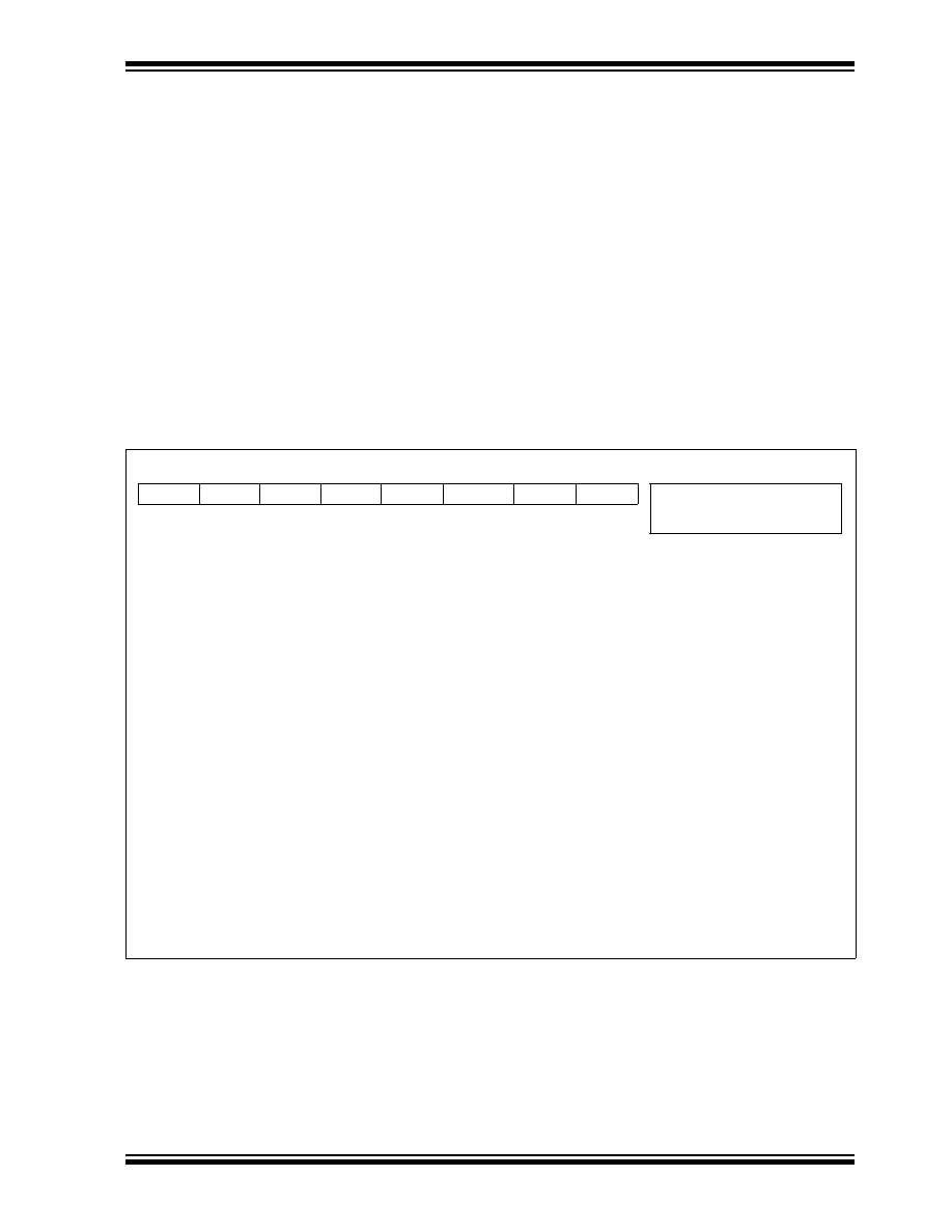
FIGURE 12-1: TCON1 REGISTER (ADDRESS: 16h, BANK 3)
R/W - 0
CA2ED1 CA2ED0 CA1ED1 CA1ED0
T16
TMR3CS TMR2CS TMR1CS
R = Readable bit
W = Writable bit
-n = Value at POR reset
bit7
bit0
bit 7-6:
CA2ED1:CA2ED0: Capture2 Mode Select bits
00 = Capture on every falling edge
01 = Capture on every rising edge
10 = Capture on every 4th rising edge
11 = Capture on every 16th rising edge
bit 5-4:
CA1ED1:CA1ED0: Capture1 Mode Select bits
00 = Capture on every falling edge
01 = Capture on every rising edge
10 = Capture on every 4th rising edge
11 = Capture on every 16th rising edge
bit 3:
T16: Timer1:Timer2 Mode Select bit
1 = Timer1 and Timer2 form a 16-bit timer
0 = Timer1 and Timer2 are two 8-bit timers
bit 2:
TMR3CS: Timer3 Clock Source Select bit
1 = TMR3 increments off the falling edge of the RB5/TCLK3 pin
0 = TMR3 increments off the internal clock
bit 1:
TMR2CS: Timer2 Clock Source Select bit
1 = TMR2 increments off the falling edge of the RB4/TCLK12 pin
0 = TMR2 increments off the internal clock
bit 0:
TMR1CS: Timer1 Clock Source Select bit
1 = TMR1 increments off the falling edge of the RB4/TCLK12 pin
0 = TMR1 increments off the internal clock
This document was created with FrameMaker404
相关PDF资料 |
PDF描述 |
|---|---|
| C8051F020R | IC 8051 MCU 64K FLASH 100TQFP |
| C8051F016R | IC 8051 MCU 32K FLASH 48TQFP |
| C8051F015R | IC 8051 MCU 32K FLASH 64TQFP |
| C8051F017R | IC 8051 MCU 32K FLASH 32LQFP |
| C8051F007R | IC 8051 MCU 32K FLASH 32LQFP |
相关代理商/技术参数 |
参数描述 |
|---|---|
| PIC18F2620T-I/SO | 功能描述:8位微控制器 -MCU 64KB 3968 RAM 25 I/O RoHS:否 制造商:Silicon Labs 核心:8051 处理器系列:C8051F39x 数据总线宽度:8 bit 最大时钟频率:50 MHz 程序存储器大小:16 KB 数据 RAM 大小:1 KB 片上 ADC:Yes 工作电源电压:1.8 V to 3.6 V 工作温度范围:- 40 C to + 105 C 封装 / 箱体:QFN-20 安装风格:SMD/SMT |
| PIC18F2680-E/SO | 功能描述:8位微控制器 -MCU 64KB 3328 RAM w/ECAN RoHS:否 制造商:Silicon Labs 核心:8051 处理器系列:C8051F39x 数据总线宽度:8 bit 最大时钟频率:50 MHz 程序存储器大小:16 KB 数据 RAM 大小:1 KB 片上 ADC:Yes 工作电源电压:1.8 V to 3.6 V 工作温度范围:- 40 C to + 105 C 封装 / 箱体:QFN-20 安装风格:SMD/SMT |
| PIC18F2680-E/SP | 功能描述:8位微控制器 -MCU 64KB 3328 RAM w/ECAN RoHS:否 制造商:Silicon Labs 核心:8051 处理器系列:C8051F39x 数据总线宽度:8 bit 最大时钟频率:50 MHz 程序存储器大小:16 KB 数据 RAM 大小:1 KB 片上 ADC:Yes 工作电源电压:1.8 V to 3.6 V 工作温度范围:- 40 C to + 105 C 封装 / 箱体:QFN-20 安装风格:SMD/SMT |
| PIC18F2680-H/SO | 功能描述:8位微控制器 -MCU 64 KB Flash 3328 RAM 25 I/O w/ECAN RoHS:否 制造商:Silicon Labs 核心:8051 处理器系列:C8051F39x 数据总线宽度:8 bit 最大时钟频率:50 MHz 程序存储器大小:16 KB 数据 RAM 大小:1 KB 片上 ADC:Yes 工作电源电压:1.8 V to 3.6 V 工作温度范围:- 40 C to + 105 C 封装 / 箱体:QFN-20 安装风格:SMD/SMT |
| PIC18F2680-H/SP | 功能描述:8位微控制器 -MCU 64 KB Flash 3328 RAM 25 I/O w/ECAN RoHS:否 制造商:Silicon Labs 核心:8051 处理器系列:C8051F39x 数据总线宽度:8 bit 最大时钟频率:50 MHz 程序存储器大小:16 KB 数据 RAM 大小:1 KB 片上 ADC:Yes 工作电源电压:1.8 V to 3.6 V 工作温度范围:- 40 C to + 105 C 封装 / 箱体:QFN-20 安装风格:SMD/SMT |
发布紧急采购,3分钟左右您将得到回复。