- 您现在的位置:买卖IC网 > PDF目录11465 > PIC18F4321-E/PT (Microchip Technology)IC PIC MCU FLASH 4KX16 44TQFP PDF资料下载
参数资料
| 型号: | PIC18F4321-E/PT |
| 厂商: | Microchip Technology |
| 文件页数: | 77/110页 |
| 文件大小: | 0K |
| 描述: | IC PIC MCU FLASH 4KX16 44TQFP |
| 产品培训模块: | Asynchronous Stimulus |
| 标准包装: | 160 |
| 系列: | PIC® 18F |
| 核心处理器: | PIC |
| 芯体尺寸: | 8-位 |
| 速度: | 25MHz |
| 连通性: | I²C,SPI,UART/USART |
| 外围设备: | 欠压检测/复位,HLVD,POR,PWM,WDT |
| 输入/输出数: | 36 |
| 程序存储器容量: | 8KB(4K x 16) |
| 程序存储器类型: | 闪存 |
| EEPROM 大小: | 256 x 8 |
| RAM 容量: | 512 x 8 |
| 电压 - 电源 (Vcc/Vdd): | 4.2 V ~ 5.5 V |
| 数据转换器: | A/D 13x10b |
| 振荡器型: | 内部 |
| 工作温度: | -40°C ~ 125°C |
| 封装/外壳: | 44-TQFP |
| 包装: | 托盘 |
第1页第2页第3页第4页第5页第6页第7页第8页第9页第10页第11页第12页第13页第14页第15页第16页第17页第18页第19页第20页第21页第22页第23页第24页第25页第26页第27页第28页第29页第30页第31页第32页第33页第34页第35页第36页第37页第38页第39页第40页第41页第42页第43页第44页第45页第46页第47页第48页第49页第50页第51页第52页第53页第54页第55页第56页第57页第58页第59页第60页第61页第62页第63页第64页第65页第66页第67页第68页第69页第70页第71页第72页第73页第74页第75页第76页当前第77页第78页第79页第80页第81页第82页第83页第84页第85页第86页第87页第88页第89页第90页第91页第92页第93页第94页第95页第96页第97页第98页第99页第100页第101页第102页第103页第104页第105页第106页第107页第108页第109页第110页
2009 Microchip Technology Inc.
DS39689F-page 69
PIC18F2221/2321/4221/4321 FAMILY
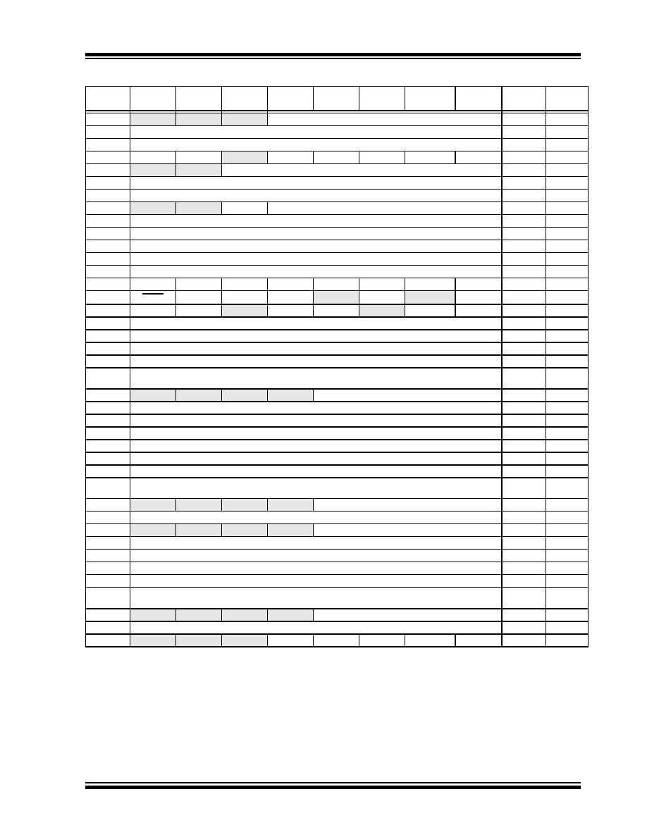
TABLE 6-2:
REGISTER FILE SUMMARY (PIC18F2221/2321/4221/4321)
File Name
Bit 7
Bit 6
Bit 5
Bit 4
Bit 3
Bit 2
Bit 1
Bit 0
Value on
POR, BOR
Details on
page:
TOSU
—
Top-of-Stack Upper Byte (TOS<20:16>)
---0 0000
TOSH
Top-of-Stack High Byte (TOS<15:8>)
0000 0000
TOSL
Top-of-Stack Low Byte (TOS<7:0>)
0000 0000
STKPTR
STKFUL(6)
STKUNF(6)
—
SP4
SP3
SP2
SP1
SP0
00-0 0000
PCLATU
—
Holding Register for PC<21:16>
--00 0000
PCLATH
Holding Register for PC<15:8>
0000 0000
PCL
PC Low Byte (PC<7:0>)
0000 0000
TBLPTRU
—
bit 21
Program Memory Table Pointer Upper Byte (TBLPTR<20:16>)
--00 0000
TBLPTRH
Program Memory Table Pointer High Byte (TBLPTR<15:8>)
0000 0000
TBLPTRL
Program Memory Table Pointer Low Byte (TBLPTR<7:0>)
0000 0000
TABLAT
Program Memory Table Latch
0000 0000
PRODH
Product Register High Byte
xxxx xxxx
PRODL
Product Register Low Byte
xxxx xxxx
INTCON
GIE/GIEH
PEIE/GIEL
TMR0IE
INT0IE
RBIE
TMR0IF
INT0IF
RBIF
0000 000x
INTCON2
RBPU
INTEDG0
INTEDG1
INTEDG2
—TMR0IP
—RBIP
1111 -1-1
INTCON3
INT2IP
INT1IP
—
INT2IE
INT1IE
—
INT2IF
INT1IF
11-0 0-00
INDF0
Uses contents of FSR0 to address data memory – value of FSR0 not changed (not a physical register)
N/A
POSTINC0 Uses contents of FSR0 to address data memory – value of FSR0 post-incremented (not a physical register)
N/A
POSTDEC0 Uses contents of FSR0 to address data memory – value of FSR0 post-decremented (not a physical register)
N/A
PREINC0
Uses contents of FSR0 to address data memory – value of FSR0 pre-incremented (not a physical register)
N/A
PLUSW0
Uses contents of FSR0 to address data memory – value of FSR0 pre-incremented (not a physical register) –
value of FSR0 offset by W
N/A
FSR0H
—
Indirect Data Memory Address Pointer 0 High Byte
---- 0000
FSR0L
Indirect Data Memory Address Pointer 0 Low Byte
xxxx xxxx
WREG
Working Register
xxxx xxxx
INDF1
Uses contents of FSR1 to address data memory – value of FSR1 not changed (not a physical register)
N/A
POSTINC1 Uses contents of FSR1 to address data memory – value of FSR1 post-incremented (not a physical register)
N/A
POSTDEC1 Uses contents of FSR1 to address data memory – value of FSR1 post-decremented (not a physical register)
N/A
PREINC1
Uses contents of FSR1 to address data memory – value of FSR1 pre-incremented (not a physical register)
N/A
PLUSW1
Uses contents of FSR1 to address data memory – value of FSR1 pre-incremented (not a physical register) –
value of FSR1 offset by W
N/A
FSR1H
—
Indirect Data Memory Address Pointer 1 High Byte
---- 0000
FSR1L
Indirect Data Memory Address Pointer 1 Low Byte
xxxx xxxx
BSR
—
Bank Select Register
---- 0000
INDF2
Uses contents of FSR2 to address data memory – value of FSR2 not changed (not a physical register)
N/A
POSTINC2 Uses contents of FSR2 to address data memory – value of FSR2 post-incremented (not a physical register)
N/A
POSTDEC2 Uses contents of FSR2 to address data memory – value of FSR2 post-decremented (not a physical register)
N/A
PREINC2
Uses contents of FSR2 to address data memory – value of FSR2 pre-incremented (not a physical register)
N/A
PLUSW2
Uses contents of FSR2 to address data memory – value of FSR2 pre-incremented (not a physical register) –
value of FSR2 offset by W
N/A
FSR2H
—
Indirect Data Memory Address Pointer 2 High Byte
---- 0000
FSR2L
Indirect Data Memory Address Pointer 2 Low Byte
xxxx xxxx
STATUS
—
—N
OV
Z
DC
C
---x xxxx
Legend:
x = unknown, u = unchanged, — = unimplemented, q = value depends on condition
Note
1:
The SBOREN bit is only available when the BOREN<1:0> Configuration bits = 01; otherwise, it is disabled and reads as ‘0’. See
2:
These registers and/or bits are not implemented on 28-pin devices and are read as ‘0’. Reset values are shown for 40/44-pin devices;
individual unimplemented bits should be interpreted as ‘-’.
3:
The PLLEN bit is only available in specific oscillator configurations; otherwise, it is disabled and reads as ‘0’. See Section 3.6.4 “PLL in
4:
The RE3 bit is only available when Master Clear Reset is disabled (MCLRE Configuration bit = 0); otherwise, RE3 reads as ‘0’. This bit is
read-only.
5:
RA6/RA7 and their associated latch and direction bits are individually configured as port pins based on various primary oscillator modes.
When disabled, these bits read as ‘0’.
6:
Bit 7 and bit 6 are cleared by user software or by a POR.
相关PDF资料 |
PDF描述 |
|---|---|
| PIC24HJ32GP204T-I/PT | IC PIC MCU FLASH 32K 44TQFP |
| GRM2196S2A1R0CD01D | CAP CER 1PF 100V S2H 0805 |
| GRM2196R2A4R7CD01D | CAP CER 4.7PF 100V R2H 0805 |
| GRM2196R2A4R3CD01D | CAP CER 4.3PF 100V R2H 0805 |
| GRM2196R2A3R9CD01D | CAP CER 3.9PF 100V R2H 0805 |
相关代理商/技术参数 |
参数描述 |
|---|---|
| PIC18F4321-I/ML | 功能描述:8位微控制器 -MCU 8 KB Flash 512 RAM RoHS:否 制造商:Silicon Labs 核心:8051 处理器系列:C8051F39x 数据总线宽度:8 bit 最大时钟频率:50 MHz 程序存储器大小:16 KB 数据 RAM 大小:1 KB 片上 ADC:Yes 工作电源电压:1.8 V to 3.6 V 工作温度范围:- 40 C to + 105 C 封装 / 箱体:QFN-20 安装风格:SMD/SMT |
| PIC18F4321-I/P | 功能描述:8位微控制器 -MCU 8 KB Flash 512 RAM RoHS:否 制造商:Silicon Labs 核心:8051 处理器系列:C8051F39x 数据总线宽度:8 bit 最大时钟频率:50 MHz 程序存储器大小:16 KB 数据 RAM 大小:1 KB 片上 ADC:Yes 工作电源电压:1.8 V to 3.6 V 工作温度范围:- 40 C to + 105 C 封装 / 箱体:QFN-20 安装风格:SMD/SMT |
| PIC18F4321-I/P | 制造商:Microchip Technology Inc 功能描述:8-Bit Microcontroller IC |
| PIC18F4321-I/PT | 功能描述:8位微控制器 -MCU 8 KB Flash 512 RAM RoHS:否 制造商:Silicon Labs 核心:8051 处理器系列:C8051F39x 数据总线宽度:8 bit 最大时钟频率:50 MHz 程序存储器大小:16 KB 数据 RAM 大小:1 KB 片上 ADC:Yes 工作电源电压:1.8 V to 3.6 V 工作温度范围:- 40 C to + 105 C 封装 / 箱体:QFN-20 安装风格:SMD/SMT |
| PIC18F4321-I/PT | 制造商:Microchip Technology Inc 功能描述:8-Bit Microcontroller IC |
发布紧急采购,3分钟左右您将得到回复。