- 您现在的位置:买卖IC网 > PDF目录299771 > PIC18F442-E/L 8-BIT, FLASH, 40 MHz, RISC MICROCONTROLLER, PQCC44 PDF资料下载
参数资料
| 型号: | PIC18F442-E/L |
| 元件分类: | 微控制器/微处理器 |
| 英文描述: | 8-BIT, FLASH, 40 MHz, RISC MICROCONTROLLER, PQCC44 |
| 封装: | PLASTIC, MO-047, LCC-44 |
| 文件页数: | 276/332页 |
| 文件大小: | 5575K |
| 代理商: | PIC18F442-E/L |
第1页第2页第3页第4页第5页第6页第7页第8页第9页第10页第11页第12页第13页第14页第15页第16页第17页第18页第19页第20页第21页第22页第23页第24页第25页第26页第27页第28页第29页第30页第31页第32页第33页第34页第35页第36页第37页第38页第39页第40页第41页第42页第43页第44页第45页第46页第47页第48页第49页第50页第51页第52页第53页第54页第55页第56页第57页第58页第59页第60页第61页第62页第63页第64页第65页第66页第67页第68页第69页第70页第71页第72页第73页第74页第75页第76页第77页第78页第79页第80页第81页第82页第83页第84页第85页第86页第87页第88页第89页第90页第91页第92页第93页第94页第95页第96页第97页第98页第99页第100页第101页第102页第103页第104页第105页第106页第107页第108页第109页第110页第111页第112页第113页第114页第115页第116页第117页第118页第119页第120页第121页第122页第123页第124页第125页第126页第127页第128页第129页第130页第131页第132页第133页第134页第135页第136页第137页第138页第139页第140页第141页第142页第143页第144页第145页第146页第147页第148页第149页第150页第151页第152页第153页第154页第155页第156页第157页第158页第159页第160页第161页第162页第163页第164页第165页第166页第167页第168页第169页第170页第171页第172页第173页第174页第175页第176页第177页第178页第179页第180页第181页第182页第183页第184页第185页第186页第187页第188页第189页第190页第191页第192页第193页第194页第195页第196页第197页第198页第199页第200页第201页第202页第203页第204页第205页第206页第207页第208页第209页第210页第211页第212页第213页第214页第215页第216页第217页第218页第219页第220页第221页第222页第223页第224页第225页第226页第227页第228页第229页第230页第231页第232页第233页第234页第235页第236页第237页第238页第239页第240页第241页第242页第243页第244页第245页第246页第247页第248页第249页第250页第251页第252页第253页第254页第255页第256页第257页第258页第259页第260页第261页第262页第263页第264页第265页第266页第267页第268页第269页第270页第271页第272页第273页第274页第275页当前第276页第277页第278页第279页第280页第281页第282页第283页第284页第285页第286页第287页第288页第289页第290页第291页第292页第293页第294页第295页第296页第297页第298页第299页第300页第301页第302页第303页第304页第305页第306页第307页第308页第309页第310页第311页第312页第313页第314页第315页第316页第317页第318页第319页第320页第321页第322页第323页第324页第325页第326页第327页第328页第329页第330页第331页第332页
PIC18FXX2
DS39564C-page 46
2006 Microchip Technology Inc.
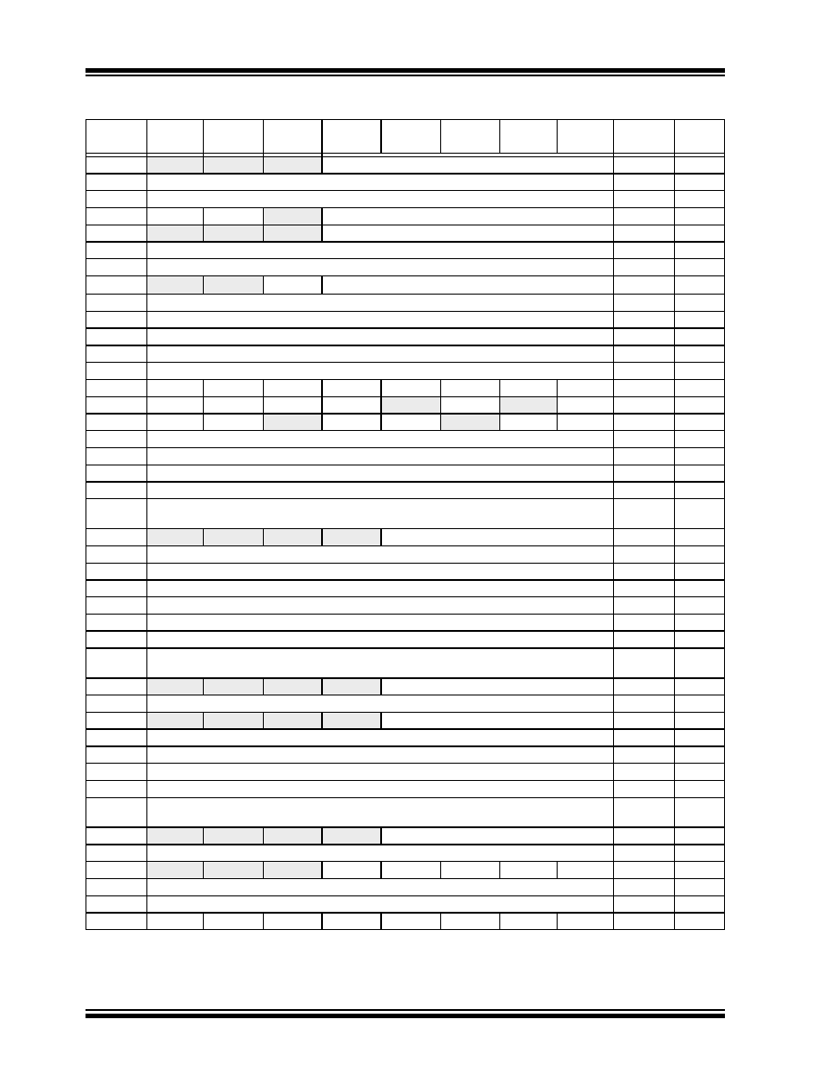
TABLE 4-2:
REGISTER FILE SUMMARY
File Name
Bit 7
Bit 6
Bit 5
Bit 4
Bit 3
Bit 2
Bit 1
Bit 0
Value on
POR, BOR
Details
on page:
TOSU
—
Top-of-Stack upper Byte (TOS<20:16>)
---0 0000
TOSH
Top-of-Stack High Byte (TOS<15:8>)
0000 0000
TOSL
Top-of-Stack Low Byte (TOS<7:0>)
0000 0000
STKPTR
STKFUL
STKUNF
—
Return Stack Pointer
00-0 0000
PCLATU
—
Holding Register for PC<20:16>
---0 0000
PCLATH
Holding Register for PC<15:8>
0000 0000
PCL
PC Low Byte (PC<7:0>)
0000 0000
TBLPTRU
—
—bit21(2)
Program Memory Table Pointer Upper Byte (TBLPTR<20:16>)
--00 0000
TBLPTRH
Program Memory Table Pointer High Byte (TBLPTR<15:8>)
0000 0000
TBLPTRL
Program Memory Table Pointer Low Byte (TBLPTR<7:0>)
0000 0000
TABLAT
Program Memory Table Latch
0000 0000
PRODH
Product Register High Byte
xxxx xxxx
PRODL
Product Register Low Byte
xxxx xxxx
INTCON
GIE/GIEH
PEIE/GIEL
TMR0IE
INT0IE
RBIE
TMR0IF
INT0IF
RBIF
0000 000x
INTCON2
RBPU
INTEDG0
INTEDG1
INTEDG2
—TMR0IP
—RBIP
1111 -1-1
INTCON3
INT2IP
INT1IP
—
INT2IE
INT1IE
—
INT2IF
INT1IF
11-0 0-00
INDF0
Uses contents of FSR0 to address data memory - value of FSR0 not changed (not a physical register)
n/a
POSTINC0
Uses contents of FSR0 to address data memory - value of FSR0 post-incremented (not a physical register)
n/a
POSTDEC0 Uses contents of FSR0 to address data memory - value of FSR0 post-decremented (not a physical register)
n/a
PREINC0
Uses contents of FSR0 to address data memory - value of FSR0 pre-incremented (not a physical register)
n/a
PLUSW0
Uses contents of FSR0 to address data memory - value of FSR0 (not a physical register).
Offset by value in WREG.
n/a
FSR0H
—
Indirect Data Memory Address Pointer 0 High Byte ---- 0000
FSR0L
Indirect Data Memory Address Pointer 0 Low Byte
xxxx xxxx
WREG
Working Register
xxxx xxxx
n/a
INDF1
Uses contents of FSR1 to address data memory - value of FSR1 not changed (not a physical register)
n/a
POSTINC1
Uses contents of FSR1 to address data memory - value of FSR1 post-incremented (not a physical register)
n/a
POSTDEC1 Uses contents of FSR1 to address data memory - value of FSR1 post-decremented (not a physical register)
n/a
PREINC1
Uses contents of FSR1 to address data memory - value of FSR1 pre-incremented (not a physical register)
n/a
PLUSW1
Uses contents of FSR1 to address data memory - value of FSR1 (not a physical register).
Offset by value in WREG.
n/a
FSR1H
—
Indirect Data Memory Address Pointer 1 High Byte ---- 0000
FSR1L
Indirect Data Memory Address Pointer 1 Low Byte
xxxx xxxx
BSR
—
Bank Select Register
---- 0000
INDF2
Uses contents of FSR2 to address data memory - value of FSR2 not changed (not a physical register)
n/a
POSTINC2
Uses contents of FSR2 to address data memory - value of FSR2 post-incremented (not a physical register)
n/a
POSTDEC2 Uses contents of FSR2 to address data memory - value of FSR2 post-decremented (not a physical register)
n/a
PREINC2
Uses contents of FSR2 to address data memory - value of FSR2 pre-incremented (not a physical register)
n/a
PLUSW2
Uses contents of FSR2 to address data memory - value of FSR2 (not a physical register).
Offset by value in WREG.
n/a
FSR2H
—
Indirect Data Memory Address Pointer 2 High Byte ---- 0000
FSR2L
Indirect Data Memory Address Pointer 2 Low Byte
xxxx xxxx
STATUS
—
—N
OV
Z
DC
C
---x xxxx
TMR0H
Timer0 Register High Byte
0000 0000
TMR0L
Timer0 Register Low Byte
xxxx xxxx
T0CON
TMR0ON
T08BIT
T0CS
T0SE
PSA
T0PS2
T0PS1
T0PS0
1111 1111
Legend:
x
= unknown, u = unchanged, - = unimplemented, q = value depends on condition
Note 1:
RA6 and associated bits are configured as port pins in RCIO and ECIO Oscillator mode only and read '0' in all other Oscillator modes.
2:
Bit 21 of the TBLPTRU allows access to the device configuration bits.
3:
These registers and bits are reserved on the PIC18F2X2 devices; always maintain these clear.
相关PDF资料 |
PDF描述 |
|---|---|
| PIC18F258I/SP | 8-BIT, FLASH, 40 MHz, RISC MICROCONTROLLER, PDIP28 |
| PIC18LF448-I/PT | 8-BIT, FLASH, 40 MHz, RISC MICROCONTROLLER, PQFP44 |
| PIC18F4539T-I/ML | 8-BIT, FLASH, 40 MHz, RISC MICROCONTROLLER, PQCC44 |
| PIC18F458TE/PTG | 8-BIT, OTPROM, 40 MHz, RISC MICROCONTROLLER, PQFP44 |
| PIC18LF1220T-I/SS | 8-BIT, FLASH, 40 MHz, RISC MICROCONTROLLER, PDSO20 |
相关代理商/技术参数 |
参数描述 |
|---|---|
| PIC18F442-I/L | 功能描述:8位微控制器 -MCU 16KB 768 RAM 34I/O RoHS:否 制造商:Silicon Labs 核心:8051 处理器系列:C8051F39x 数据总线宽度:8 bit 最大时钟频率:50 MHz 程序存储器大小:16 KB 数据 RAM 大小:1 KB 片上 ADC:Yes 工作电源电压:1.8 V to 3.6 V 工作温度范围:- 40 C to + 105 C 封装 / 箱体:QFN-20 安装风格:SMD/SMT |
| PIC18F442-I/L | 制造商:Microchip Technology Inc 功能描述:8BIT FLASH MCU SMD 18F442 PLCC44 |
| PIC18F442-I/ML | 功能描述:8位微控制器 -MCU 16KB 768 RAM 34I/O RoHS:否 制造商:Silicon Labs 核心:8051 处理器系列:C8051F39x 数据总线宽度:8 bit 最大时钟频率:50 MHz 程序存储器大小:16 KB 数据 RAM 大小:1 KB 片上 ADC:Yes 工作电源电压:1.8 V to 3.6 V 工作温度范围:- 40 C to + 105 C 封装 / 箱体:QFN-20 安装风格:SMD/SMT |
| PIC18F442-I/P | 功能描述:8位微控制器 -MCU 16KB 768 RAM 34I/O RoHS:否 制造商:Silicon Labs 核心:8051 处理器系列:C8051F39x 数据总线宽度:8 bit 最大时钟频率:50 MHz 程序存储器大小:16 KB 数据 RAM 大小:1 KB 片上 ADC:Yes 工作电源电压:1.8 V to 3.6 V 工作温度范围:- 40 C to + 105 C 封装 / 箱体:QFN-20 安装风格:SMD/SMT |
| PIC18F442-I/P | 制造商:Microchip Technology Inc 功能描述:IC 8BIT FLASH MCU 18F442 DIP40 |
发布紧急采购,3分钟左右您将得到回复。