- 您现在的位置:买卖IC网 > PDF目录11308 > PIC18F442T-I/PT (Microchip Technology)IC MCU FLASH 8KX16 EE A/D 44TQFP PDF资料下载
参数资料
| 型号: | PIC18F442T-I/PT |
| 厂商: | Microchip Technology |
| 文件页数: | 123/134页 |
| 文件大小: | 0K |
| 描述: | IC MCU FLASH 8KX16 EE A/D 44TQFP |
| 产品培训模块: | Asynchronous Stimulus |
| 标准包装: | 1,200 |
| 系列: | PIC® 18F |
| 核心处理器: | PIC |
| 芯体尺寸: | 8-位 |
| 速度: | 40MHz |
| 连通性: | I²C,SPI,UART/USART |
| 外围设备: | 欠压检测/复位,LVD,POR,PWM,WDT |
| 输入/输出数: | 34 |
| 程序存储器容量: | 16KB(8K x 16) |
| 程序存储器类型: | 闪存 |
| EEPROM 大小: | 256 x 8 |
| RAM 容量: | 768 x 8 |
| 电压 - 电源 (Vcc/Vdd): | 4.2 V ~ 5.5 V |
| 数据转换器: | A/D 8x10b |
| 振荡器型: | 外部 |
| 工作温度: | -40°C ~ 85°C |
| 封装/外壳: | 44-TQFP |
| 包装: | 带卷 (TR) |
第1页第2页第3页第4页第5页第6页第7页第8页第9页第10页第11页第12页第13页第14页第15页第16页第17页第18页第19页第20页第21页第22页第23页第24页第25页第26页第27页第28页第29页第30页第31页第32页第33页第34页第35页第36页第37页第38页第39页第40页第41页第42页第43页第44页第45页第46页第47页第48页第49页第50页第51页第52页第53页第54页第55页第56页第57页第58页第59页第60页第61页第62页第63页第64页第65页第66页第67页第68页第69页第70页第71页第72页第73页第74页第75页第76页第77页第78页第79页第80页第81页第82页第83页第84页第85页第86页第87页第88页第89页第90页第91页第92页第93页第94页第95页第96页第97页第98页第99页第100页第101页第102页第103页第104页第105页第106页第107页第108页第109页第110页第111页第112页第113页第114页第115页第116页第117页第118页第119页第120页第121页第122页当前第123页第124页第125页第126页第127页第128页第129页第130页第131页第132页第133页第134页
1997 Microchip Technology Inc.
DS30444E - page 89
PIC16C9XX
13.0
LCD MODULE
The LCD module generates the timing control to drive
a static or multiplexed LCD panel, with support for up to
32 segments multiplexed with up to 4 commons. It also
provides control of the LCD pixel data.
The interface to the module consists of 3 control regis-
ters (LCDCON, LCDSE, and LCDPS) used to dene
the timing requirements of the LCD panel and up to 16
LCD data registers (LCD00-LCD15) that represent the
array of the pixel data. In normal operation, the control
registers are congured to match the LCD panel being
used. Primarily, the initialization information consists of
selecting the number of commons required by the LCD
panel, and then specifying the LCD Frame clock rate to
be used by the panel.
Once the module is initialized for the LCD panel, the
individual bits of the LCD data registers are cleared/set
to represent a clear/dark pixel respectively.
Once
the
module
is
congured,
the
LCDEN
(LCDCON<7>) bit is used to enable or disable the LCD
module. The LCD panel can also operate during sleep
by clearing the SLPEN (LCDCON<6>) bit.
Figure 13-4 through Figure 13-7 provides waveforms
for Static, 1/2, 1/3, and 1/4 MUX drives.
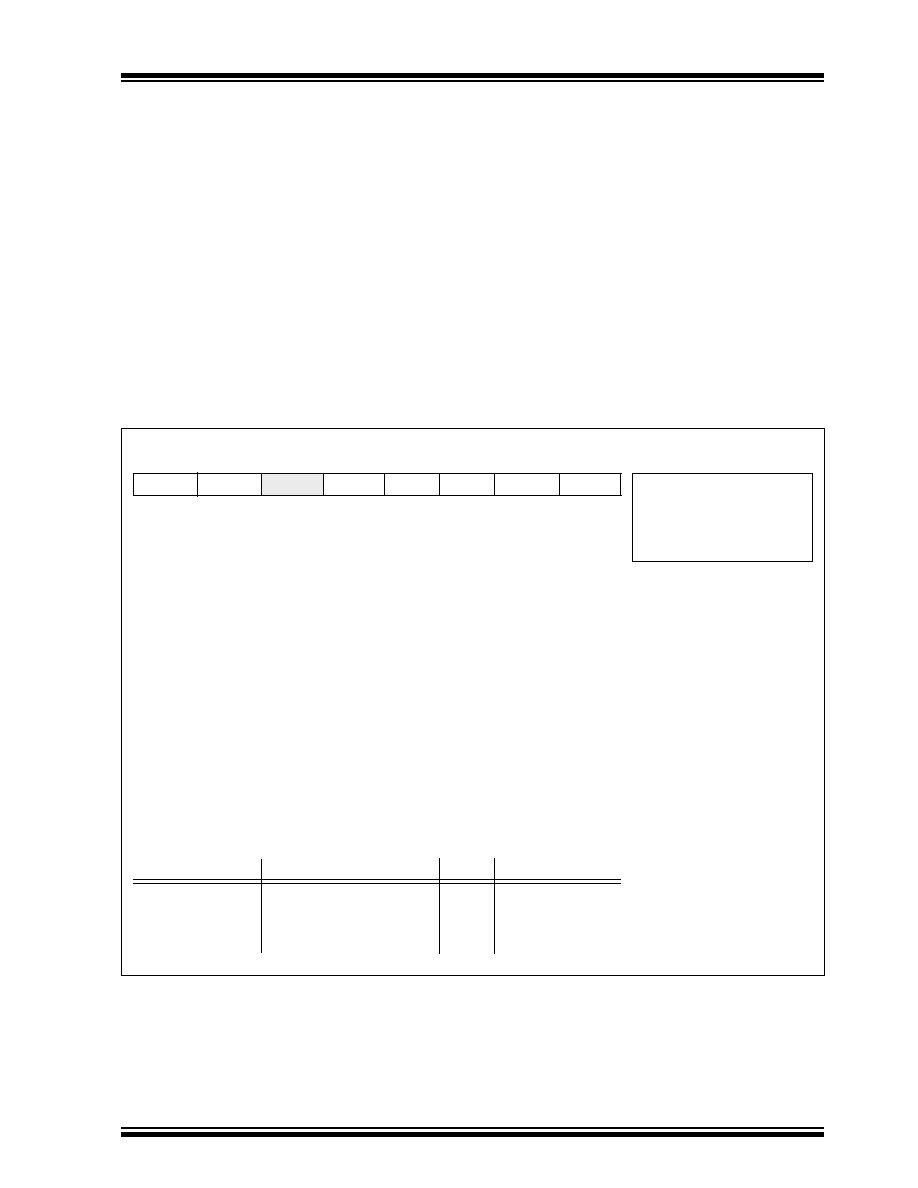
FIGURE 13-1: LCDCON REGISTER (ADDRESS 10Fh)
R/W-0
U-0
R/W-0
LCDEN
SLPEN
—
VGEN
CS1
CS0
LMUX1
LMUX0
R =Readable bit
W =Writable bit
U =Unimplemented bit,
Read as ‘0’
-n =Value at POR reset
bit7
bit0
bit 7:
LCDEN: Module drive enable bit
1 = LCD drive enabled
0 = LCD drive disabled
bit 6:
SLPEN: LCD display sleep enable
1 = LCD module will stop operating during SLEEP
0 = LCD module will continue to display during SLEEP
bit 5:
Unimplemented: Read as '0'
bit 4:
VGEN: Voltage Generator Enable
1 = Internal LCD Voltage Generator Enabled, (powered-up)
0 = Internal LCD Voltage Generator powered-down, voltage is expected to be provided externally
bit 3-2: CS1:CS0: Clock Source Select bits
00 = Fosc/256
01 = T1CKI (Timer1)
1x = Internal RC oscillator
bit 1-0:
LMUX1:LMUX0: Common Selection bits
Species the number of commons and the bias method
LMUX1:LMUX0
MULTIPLEX
BIAS
Max # of Segments
00
01
10
11
Static (COM0)
1/2
(COM0, 1)
1/3
(COM0, 1, 2)
1/4
(COM0, 1, 2, 3)
Static
1/3
32
31
30
29
相关PDF资料 |
PDF描述 |
|---|---|
| RPE5C1H1R0C2S1B03A | CAP CER 1PF 50V RADIAL |
| PIC24FJ256GB210T-I/BG | MCU 16BIT 256K FLASH 121-BGA |
| RPE5C1H180J2S1Z03A | CAP CER 18PF 50V 5% RADIAL |
| RPE5C1H150J2S1Z03A | CAP CER 15PF 50V 5% RADIAL |
| PIC24HJ256GP210A-E/PF | MCU 16BIT 256K FLASH 100TQFP |
相关代理商/技术参数 |
参数描述 |
|---|---|
| PIC18F4431-E/ML | 功能描述:8位微控制器 -MCU 16KB 768 RAM 34 I/O RoHS:否 制造商:Silicon Labs 核心:8051 处理器系列:C8051F39x 数据总线宽度:8 bit 最大时钟频率:50 MHz 程序存储器大小:16 KB 数据 RAM 大小:1 KB 片上 ADC:Yes 工作电源电压:1.8 V to 3.6 V 工作温度范围:- 40 C to + 105 C 封装 / 箱体:QFN-20 安装风格:SMD/SMT |
| PIC18F4431-E/P | 功能描述:8位微控制器 -MCU 16KB 768 RAM 34 I/O RoHS:否 制造商:Silicon Labs 核心:8051 处理器系列:C8051F39x 数据总线宽度:8 bit 最大时钟频率:50 MHz 程序存储器大小:16 KB 数据 RAM 大小:1 KB 片上 ADC:Yes 工作电源电压:1.8 V to 3.6 V 工作温度范围:- 40 C to + 105 C 封装 / 箱体:QFN-20 安装风格:SMD/SMT |
| PIC18F4431-E/P | 制造商:Microchip Technology Inc 功能描述:IC 8BIT FLASH MCU 18F4431 DIP40 |
| PIC18F4431-E/PT | 功能描述:8位微控制器 -MCU 16KB 768 RAM 34 I/O RoHS:否 制造商:Silicon Labs 核心:8051 处理器系列:C8051F39x 数据总线宽度:8 bit 最大时钟频率:50 MHz 程序存储器大小:16 KB 数据 RAM 大小:1 KB 片上 ADC:Yes 工作电源电压:1.8 V to 3.6 V 工作温度范围:- 40 C to + 105 C 封装 / 箱体:QFN-20 安装风格:SMD/SMT |
| PIC18F4431-E/PT | 制造商:Microchip Technology Inc 功能描述:IC 8BIT FLASH MCU 18F4431 TQFP44 |
发布紧急采购,3分钟左右您将得到回复。