- 您现在的位置:买卖IC网 > PDF目录224776 > PIC18F4450-E/P 8-BIT, FLASH, 48 MHz, MICROCONTROLLER, PDIP40 PDF资料下载
参数资料
| 型号: | PIC18F4450-E/P |
| 元件分类: | 微控制器/微处理器 |
| 英文描述: | 8-BIT, FLASH, 48 MHz, MICROCONTROLLER, PDIP40 |
| 封装: | 0.600 INCH, LEAD FREE, PLASTIC, DIP-40 |
| 文件页数: | 50/324页 |
| 文件大小: | 5672K |
| 代理商: | PIC18F4450-E/P |
第1页第2页第3页第4页第5页第6页第7页第8页第9页第10页第11页第12页第13页第14页第15页第16页第17页第18页第19页第20页第21页第22页第23页第24页第25页第26页第27页第28页第29页第30页第31页第32页第33页第34页第35页第36页第37页第38页第39页第40页第41页第42页第43页第44页第45页第46页第47页第48页第49页当前第50页第51页第52页第53页第54页第55页第56页第57页第58页第59页第60页第61页第62页第63页第64页第65页第66页第67页第68页第69页第70页第71页第72页第73页第74页第75页第76页第77页第78页第79页第80页第81页第82页第83页第84页第85页第86页第87页第88页第89页第90页第91页第92页第93页第94页第95页第96页第97页第98页第99页第100页第101页第102页第103页第104页第105页第106页第107页第108页第109页第110页第111页第112页第113页第114页第115页第116页第117页第118页第119页第120页第121页第122页第123页第124页第125页第126页第127页第128页第129页第130页第131页第132页第133页第134页第135页第136页第137页第138页第139页第140页第141页第142页第143页第144页第145页第146页第147页第148页第149页第150页第151页第152页第153页第154页第155页第156页第157页第158页第159页第160页第161页第162页第163页第164页第165页第166页第167页第168页第169页第170页第171页第172页第173页第174页第175页第176页第177页第178页第179页第180页第181页第182页第183页第184页第185页第186页第187页第188页第189页第190页第191页第192页第193页第194页第195页第196页第197页第198页第199页第200页第201页第202页第203页第204页第205页第206页第207页第208页第209页第210页第211页第212页第213页第214页第215页第216页第217页第218页第219页第220页第221页第222页第223页第224页第225页第226页第227页第228页第229页第230页第231页第232页第233页第234页第235页第236页第237页第238页第239页第240页第241页第242页第243页第244页第245页第246页第247页第248页第249页第250页第251页第252页第253页第254页第255页第256页第257页第258页第259页第260页第261页第262页第263页第264页第265页第266页第267页第268页第269页第270页第271页第272页第273页第274页第275页第276页第277页第278页第279页第280页第281页第282页第283页第284页第285页第286页第287页第288页第289页第290页第291页第292页第293页第294页第295页第296页第297页第298页第299页第300页第301页第302页第303页第304页第305页第306页第307页第308页第309页第310页第311页第312页第313页第314页第315页第316页第317页第318页第319页第320页第321页第322页第323页第324页
PIC18F2450/4450
2008 Microchip Technology Inc.
DS39760D-page 141
14.4.4
PING-PONG BUFFERING
An endpoint is defined to have a ping-pong buffer when
it has two sets of BD entries: one set for an EVEN
transfer and one set for an ODD transfer. This allows
the CPU to process one BD while the SIE is processing
the other BD. Double-buffering BDs in this way allows
for maximum throughput to/from the USB.
The USB module supports three modes of operation:
No ping-pong support
Ping-pong buffer support for OUT Endpoint 0 only
Ping-pong buffer support for all endpoints
The ping-pong buffer settings are configured using the
PPB1:PPB0 bits in the UCFG register.
The USB module keeps track of the Ping-Pong Pointer
individually for each endpoint. All pointers are initially
reset to the EVEN BD when the module is enabled.
After the completion of a transaction (UOWN cleared
by the SIE), the pointer is toggled to the ODD BD. After
the completion of the next transaction, the pointer is
toggled back to the EVEN BD and so on.
The EVEN/ODD status of the last transaction is stored
in the PPBI bit of the USTAT register. The user can
reset all Ping-Pong Pointers to EVEN using the
PPBRST bit.
Figure 14-7 shows the three different modes of
operation and how USB RAM is filled with the BDs.
BDs have a fixed relationship to a particular endpoint,
depending on the buffering configuration. The mapping
of BDs to endpoints is detailed in Table 14-4. This
relationship also means that gaps may occur in the
BDT if endpoints are not enabled contiguously. This
theoretically means that the BDs for disabled endpoints
could be used as buffer space. In practice, users
should avoid using such spaces in the BDT unless a
method of validating BD addresses is implemented.
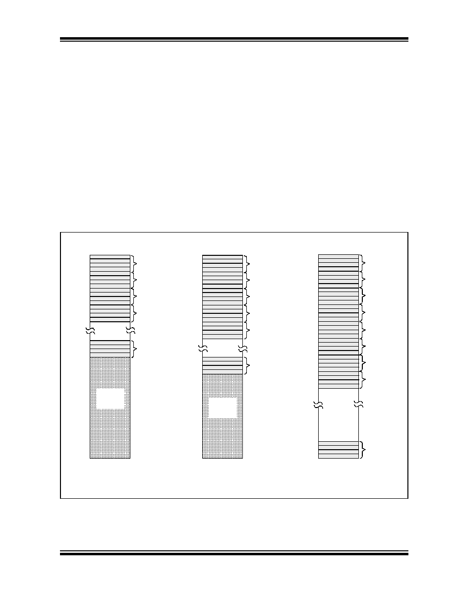
FIGURE 14-7:
BUFFER DESCRIPTOR TABLE MAPPING FOR BUFFERING MODES
EP1 IN EVEN
EP1 OUT EVEN
EP1 OUT ODD
EP1 IN ODD
Descriptor
EP1 IN
EP15 IN
EP1 OUT
EP0 OUT
PPB1:PPB0 = 00
EP0 IN
EP1 IN
No Ping-Pong Buffers
EP15 IN
EP0 IN
EP0 OUT EVEN
PPB1:PPB0 = 01
EP0 OUT ODD
EP1 OUT
Ping-Pong Buffer on EP0 OUT
EP15 IN ODD
EP0 IN EVEN
EP0 OUT EVEN
PPB1:PPB0 = 10
EP0 OUT ODD
EP0 IN ODD
Ping-Pong Buffers on All EPs
Descriptor
400h
4FFh
400h
47Fh
483h
Available
as
Data RAM
Available
as
Data RAM
Maximum Memory Used: 128 bytes
Maximum BDs: 32 (BD0 to BD31)
Maximum Memory Used: 132 bytes
Maximum BDs: 33 (BD0 to BD32)
Maximum Memory Used: 256 bytes
Maximum BDs: 64 (BD0 to BD63)
Note:
Memory area not shown to scale.
Descriptor
相关PDF资料 |
PDF描述 |
|---|---|
| PIC18F4450T-E/PT | 8-BIT, FLASH, 48 MHz, MICROCONTROLLER, PQFP44 |
| PIC18LF24J10-E/PT | 8-BIT, FLASH, 40 MHz, RISC MICROCONTROLLER, PQFP44 |
| PID1309 | Single Resistor Gain Programmable, Precision Instrumentation Amplifier; Package: PDIP; No of Pins: 8; Temperature Range: 0°C to +70°C |
| PID1501 | 1A, 1.2MHz/2.2MHz, Step-Up DC/DC Converters in ThinSOT; Package: SOT; No of Pins: 5; Temperature Range: -40°C to +125°C |
| PID1602 | Interface IC |
相关代理商/技术参数 |
参数描述 |
|---|---|
| PIC18F4450-I/ML | 功能描述:8位微控制器 -MCU 16KB FL 768 RAM 34 I/O FS-USB 2.0 RoHS:否 制造商:Silicon Labs 核心:8051 处理器系列:C8051F39x 数据总线宽度:8 bit 最大时钟频率:50 MHz 程序存储器大小:16 KB 数据 RAM 大小:1 KB 片上 ADC:Yes 工作电源电压:1.8 V to 3.6 V 工作温度范围:- 40 C to + 105 C 封装 / 箱体:QFN-20 安装风格:SMD/SMT |
| PIC18F4450-I/P | 功能描述:8位微控制器 -MCU 16KB FL 768 RAM 34 I/O FS-USB 2.0 RoHS:否 制造商:Silicon Labs 核心:8051 处理器系列:C8051F39x 数据总线宽度:8 bit 最大时钟频率:50 MHz 程序存储器大小:16 KB 数据 RAM 大小:1 KB 片上 ADC:Yes 工作电源电压:1.8 V to 3.6 V 工作温度范围:- 40 C to + 105 C 封装 / 箱体:QFN-20 安装风格:SMD/SMT |
| PIC18F4450-I/PT | 功能描述:8位微控制器 -MCU 16KB FL 768 RAM 34 I/O FS-USB 2.0 RoHS:否 制造商:Silicon Labs 核心:8051 处理器系列:C8051F39x 数据总线宽度:8 bit 最大时钟频率:50 MHz 程序存储器大小:16 KB 数据 RAM 大小:1 KB 片上 ADC:Yes 工作电源电压:1.8 V to 3.6 V 工作温度范围:- 40 C to + 105 C 封装 / 箱体:QFN-20 安装风格:SMD/SMT |
| PIC18F4450T-I/ML | 功能描述:8位微控制器 -MCU 16KB FL 768 RAM 34 I/O FS-USB 2.0 RoHS:否 制造商:Silicon Labs 核心:8051 处理器系列:C8051F39x 数据总线宽度:8 bit 最大时钟频率:50 MHz 程序存储器大小:16 KB 数据 RAM 大小:1 KB 片上 ADC:Yes 工作电源电压:1.8 V to 3.6 V 工作温度范围:- 40 C to + 105 C 封装 / 箱体:QFN-20 安装风格:SMD/SMT |
| PIC18F4450T-I/PT | 功能描述:8位微控制器 -MCU 16KB FL 768 RAM 34 I/O FS-USB 2.0 RoHS:否 制造商:Silicon Labs 核心:8051 处理器系列:C8051F39x 数据总线宽度:8 bit 最大时钟频率:50 MHz 程序存储器大小:16 KB 数据 RAM 大小:1 KB 片上 ADC:Yes 工作电源电压:1.8 V to 3.6 V 工作温度范围:- 40 C to + 105 C 封装 / 箱体:QFN-20 安装风格:SMD/SMT |
发布紧急采购,3分钟左右您将得到回复。