- 您现在的位置:买卖IC网 > PDF目录3827 > PIC18F4550-I/PT (Microchip Technology)IC PIC MCU FLASH 16KX16 44TQFP PDF资料下载
参数资料
| 型号: | PIC18F4550-I/PT |
| 厂商: | Microchip Technology |
| 文件页数: | 77/438页 |
| 文件大小: | 0K |
| 描述: | IC PIC MCU FLASH 16KX16 44TQFP |
| 产品培训模块: | Asynchronous Stimulus PIC18 J Series MCU Overview 8-bit PIC® Microcontroller Portfolio |
| 标准包装: | 160 |
| 系列: | PIC® 18F |
| 核心处理器: | PIC |
| 芯体尺寸: | 8-位 |
| 速度: | 48MHz |
| 连通性: | I²C,SPI,UART/USART,USB |
| 外围设备: | 欠压检测/复位,HLVD,POR,PWM,WDT |
| 输入/输出数: | 35 |
| 程序存储器容量: | 32KB(16K x 16) |
| 程序存储器类型: | 闪存 |
| EEPROM 大小: | 256 x 8 |
| RAM 容量: | 2K x 8 |
| 电压 - 电源 (Vcc/Vdd): | 4.2 V ~ 5.5 V |
| 数据转换器: | A/D 13x10b |
| 振荡器型: | 内部 |
| 工作温度: | -40°C ~ 85°C |
| 封装/外壳: | 44-TQFP |
| 包装: | 托盘 |
| 产品目录页面: | 646 (CN2011-ZH PDF) |
| 配用: | GPIODM-KPLCD-ND - BOARD DEMO LCD GPIO EXP KEYPAD XLT44PT3-ND - SOCKET TRAN ICE 44MQFP/TQFP I3-DB18F4550-ND - BOARD DAUGHTER ICEPIC3 DM163025-ND - PIC DEM FULL SPEED USB DEMO BRD AC164305-ND - MODULE SKT FOR PM3 44TQFP 444-1001-ND - DEMO BOARD FOR PICMICRO MCU AC164020-ND - MODULE SKT PROMATEII 44TQFP |
第1页第2页第3页第4页第5页第6页第7页第8页第9页第10页第11页第12页第13页第14页第15页第16页第17页第18页第19页第20页第21页第22页第23页第24页第25页第26页第27页第28页第29页第30页第31页第32页第33页第34页第35页第36页第37页第38页第39页第40页第41页第42页第43页第44页第45页第46页第47页第48页第49页第50页第51页第52页第53页第54页第55页第56页第57页第58页第59页第60页第61页第62页第63页第64页第65页第66页第67页第68页第69页第70页第71页第72页第73页第74页第75页第76页当前第77页第78页第79页第80页第81页第82页第83页第84页第85页第86页第87页第88页第89页第90页第91页第92页第93页第94页第95页第96页第97页第98页第99页第100页第101页第102页第103页第104页第105页第106页第107页第108页第109页第110页第111页第112页第113页第114页第115页第116页第117页第118页第119页第120页第121页第122页第123页第124页第125页第126页第127页第128页第129页第130页第131页第132页第133页第134页第135页第136页第137页第138页第139页第140页第141页第142页第143页第144页第145页第146页第147页第148页第149页第150页第151页第152页第153页第154页第155页第156页第157页第158页第159页第160页第161页第162页第163页第164页第165页第166页第167页第168页第169页第170页第171页第172页第173页第174页第175页第176页第177页第178页第179页第180页第181页第182页第183页第184页第185页第186页第187页第188页第189页第190页第191页第192页第193页第194页第195页第196页第197页第198页第199页第200页第201页第202页第203页第204页第205页第206页第207页第208页第209页第210页第211页第212页第213页第214页第215页第216页第217页第218页第219页第220页第221页第222页第223页第224页第225页第226页第227页第228页第229页第230页第231页第232页第233页第234页第235页第236页第237页第238页第239页第240页第241页第242页第243页第244页第245页第246页第247页第248页第249页第250页第251页第252页第253页第254页第255页第256页第257页第258页第259页第260页第261页第262页第263页第264页第265页第266页第267页第268页第269页第270页第271页第272页第273页第274页第275页第276页第277页第278页第279页第280页第281页第282页第283页第284页第285页第286页第287页第288页第289页第290页第291页第292页第293页第294页第295页第296页第297页第298页第299页第300页第301页第302页第303页第304页第305页第306页第307页第308页第309页第310页第311页第312页第313页第314页第315页第316页第317页第318页第319页第320页第321页第322页第323页第324页第325页第326页第327页第328页第329页第330页第331页第332页第333页第334页第335页第336页第337页第338页第339页第340页第341页第342页第343页第344页第345页第346页第347页第348页第349页第350页第351页第352页第353页第354页第355页第356页第357页第358页第359页第360页第361页第362页第363页第364页第365页第366页第367页第368页第369页第370页第371页第372页第373页第374页第375页第376页第377页第378页第379页第380页第381页第382页第383页第384页第385页第386页第387页第388页第389页第390页第391页第392页第393页第394页第395页第396页第397页第398页第399页第400页第401页第402页第403页第404页第405页第406页第407页第408页第409页第410页第411页第412页第413页第414页第415页第416页第417页第418页第419页第420页第421页第422页第423页第424页第425页第426页第427页第428页第429页第430页第431页第432页第433页第434页第435页第436页第437页第438页
PIC18F2455/2550/4455/4550
DS39632E-page 166
2009 Microchip Technology Inc.
17.2
USB Status and Control
The operation of the USB module is configured and
managed through three control registers. In addition, a
total of 22 registers are used to manage the actual USB
transactions. The registers are:
USB Control register (UCON)
USB Configuration register (UCFG)
USB Transfer Status register (USTAT)
USB Device Address register (UADDR)
Frame Number registers (UFRMH:UFRML)
Endpoint Enable registers 0 through 15 (UEPn)
17.2.1
USB CONTROL REGISTER (UCON)
The USB Control register (Register 17-1) contains bits
needed to control the module behavior during transfers.
The register contains bits that control the following:
Main USB Peripheral Enable
Ping-Pong Buffer Pointer Reset
Control of the Suspend mode
Packet Transfer Disable
In addition, the USB Control register contains a status bit,
SE0 (UCON<5>), which is used to indicate the occur-
rence of a single-ended zero on the bus. When the USB
module is enabled, this bit should be monitored to deter-
mine whether the differential data lines have come out of
a single-ended zero condition. This helps to differentiate
the initial power-up state from the USB Reset signal.
The overall operation of the USB module is controlled by
the USBEN bit (UCON<3>). Setting this bit activates the
module and resets all of the PPBI bits in the Buffer
Descriptor Table to ‘0’. This bit also activates the on-chip
voltage regulator (if the VREGEN Configuration bit is
set) and connects internal pull-up resistors, if they are
enabled. Thus, this bit can be used as a soft
attach/detach to the USB. Although all status and control
bits are ignored when this bit is clear, the module needs
to be fully preconfigured prior to setting this bit.
Note:
When disabling the USB module, make
sure the SUSPND bit (UCON<1>) is clear
prior to clearing the USBEN bit. Clearing
the USBEN bit when the module is in the
suspended state may prevent the module
from fully powering down.
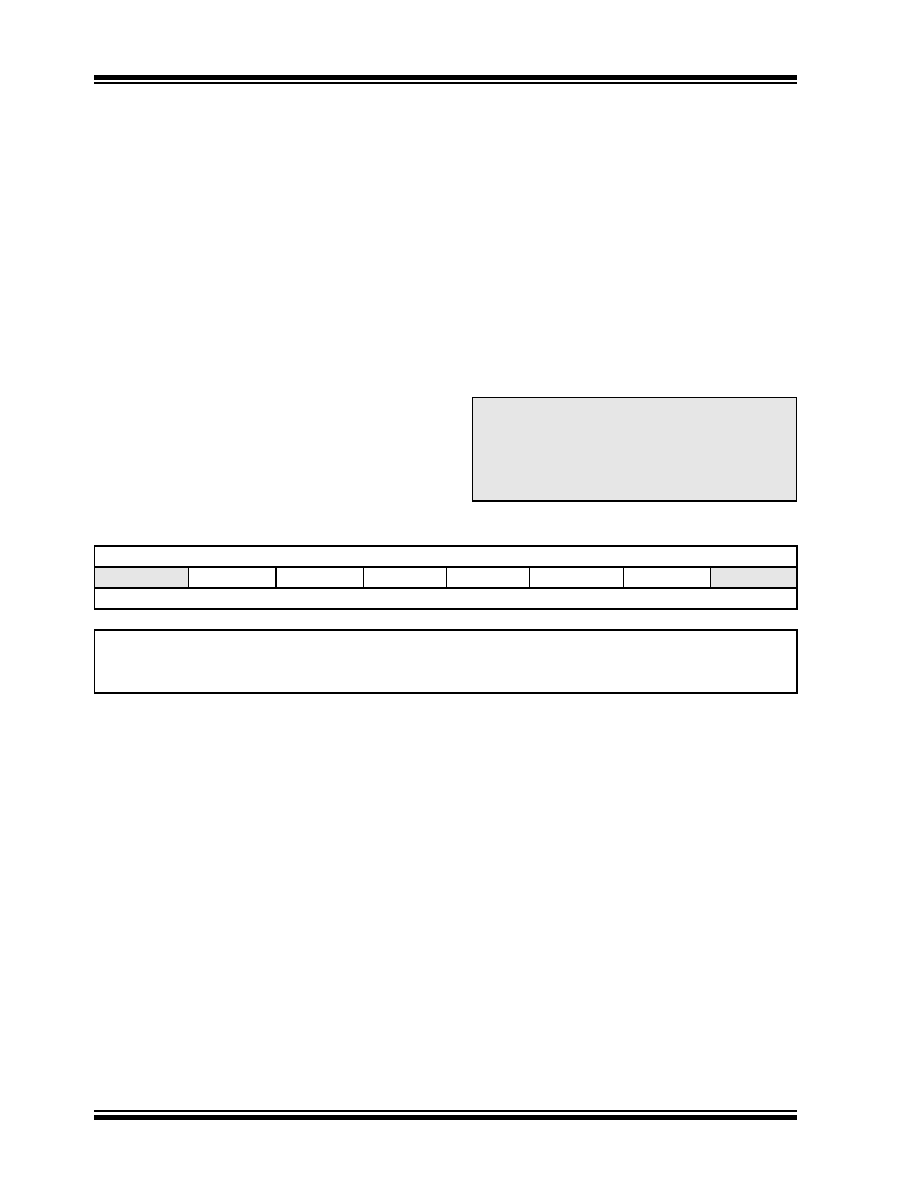
REGISTER 17-1:
UCON: USB CONTROL REGISTER
U-0
R/W-0
R-x
R/C-0
R/W-0
U-0
—
PPBRST
SE0
PKTDIS
USBEN
RESUME
SUSPND
—
bit 7
bit 0
Legend:
C = Clearable bit
R = Readable bit
W = Writable bit
U = Unimplemented bit, read as ‘0’
-n = Value at POR
‘1’ = Bit is set
‘0’ = Bit is cleared
x = Bit is unknown
bit 7
Unimplemented: Read as ‘0’
bit 6
PPBRST: Ping-Pong Buffers Reset bit
1 = Reset all Ping-Pong Buffer Pointers to the Even Buffer Descriptor (BD) banks
0 = Ping-Pong Buffer Pointers not being reset
bit 5
SE0: Live Single-Ended Zero Flag bit
1 = Single-ended zero active on the USB bus
0 = No single-ended zero detected
bit 4
PKTDIS: Packet Transfer Disable bit
1 = SIE token and packet processing disabled, automatically set when a SETUP token is received
0 = SIE token and packet processing enabled
bit 3
USBEN: USB Module Enable bit
1 = USB module and supporting circuitry enabled (device attached)
0 = USB module and supporting circuitry disabled (device detached)
bit 2
RESUME: Resume Signaling Enable bit
1 = Resume signaling activated
0 = Resume signaling disabled
bit 1
SUSPND: Suspend USB bit
1 = USB module and supporting circuitry in Power Conserve mode, SIE clock inactive
0 = USB module and supporting circuitry in normal operation, SIE clock clocked at the configured rate
bit 0
Unimplemented: Read as ‘0’
相关PDF资料 |
PDF描述 |
|---|---|
| PIC18LF2523-I/SO | IC PIC MCU FLASH 16KX16 28SOIC |
| PIC18LF4331-I/PT | IC PIC MCU FLASH 4KX16 44TQFP |
| PIC18F4331-I/ML | IC PIC MCU FLASH 4KX16 44QFN |
| PIC18F2523-I/ML | IC PIC MCU FLASH 16KX16 28QFN |
| PIC18LF4520-I/P | IC MCU FLASH 16KX16 40DIP |
相关代理商/技术参数 |
参数描述 |
|---|---|
| PIC18F4550T-I/ML | 功能描述:8位微控制器 -MCU 32kBF 2048RM FSUSB2 RoHS:否 制造商:Silicon Labs 核心:8051 处理器系列:C8051F39x 数据总线宽度:8 bit 最大时钟频率:50 MHz 程序存储器大小:16 KB 数据 RAM 大小:1 KB 片上 ADC:Yes 工作电源电压:1.8 V to 3.6 V 工作温度范围:- 40 C to + 105 C 封装 / 箱体:QFN-20 安装风格:SMD/SMT |
| PIC18F4550T-I/PT | 功能描述:8位微控制器 -MCU 32kBF 2048RM FSUSB2 RoHS:否 制造商:Silicon Labs 核心:8051 处理器系列:C8051F39x 数据总线宽度:8 bit 最大时钟频率:50 MHz 程序存储器大小:16 KB 数据 RAM 大小:1 KB 片上 ADC:Yes 工作电源电压:1.8 V to 3.6 V 工作温度范围:- 40 C to + 105 C 封装 / 箱体:QFN-20 安装风格:SMD/SMT |
| PIC18F4553-I/ML | 功能描述:8位微控制器 -MCU 32KB FLSH 2048 RAM FSUSB 2.0 12B ADC RoHS:否 制造商:Silicon Labs 核心:8051 处理器系列:C8051F39x 数据总线宽度:8 bit 最大时钟频率:50 MHz 程序存储器大小:16 KB 数据 RAM 大小:1 KB 片上 ADC:Yes 工作电源电压:1.8 V to 3.6 V 工作温度范围:- 40 C to + 105 C 封装 / 箱体:QFN-20 安装风格:SMD/SMT |
| PIC18F4553-I/P | 功能描述:8位微控制器 -MCU 32KB FLSH 2048 RAM FSUSB 2.0 12B ADC RoHS:否 制造商:Silicon Labs 核心:8051 处理器系列:C8051F39x 数据总线宽度:8 bit 最大时钟频率:50 MHz 程序存储器大小:16 KB 数据 RAM 大小:1 KB 片上 ADC:Yes 工作电源电压:1.8 V to 3.6 V 工作温度范围:- 40 C to + 105 C 封装 / 箱体:QFN-20 安装风格:SMD/SMT |
| PIC18F4553-I/P | 制造商:Microchip Technology Inc 功能描述:8-Bit Microcontroller IC |
发布紧急采购,3分钟左右您将得到回复。