- 您现在的位置:买卖IC网 > PDF目录11551 > PIC18F45K20T-I/MV (Microchip Technology)MCU 32KB FLASH 1536B RAM 40UQFN PDF资料下载
参数资料
| 型号: | PIC18F45K20T-I/MV |
| 厂商: | Microchip Technology |
| 文件页数: | 94/234页 |
| 文件大小: | 0K |
| 描述: | MCU 32KB FLASH 1536B RAM 40UQFN |
| 标准包装: | 3,300 |
| 系列: | PIC® XLP™ 18F |
| 核心处理器: | PIC |
| 芯体尺寸: | 8-位 |
| 速度: | 64MHz |
| 连通性: | I²C,SPI,UART/USART |
| 外围设备: | 欠压检测/复位,HLVD,POR,PWM,WDT |
| 输入/输出数: | 35 |
| 程序存储器容量: | 32KB(16K x 16) |
| 程序存储器类型: | 闪存 |
| EEPROM 大小: | 256 x 8 |
| RAM 容量: | 1.5K x 8 |
| 电压 - 电源 (Vcc/Vdd): | 1.8 V ~ 3.6 V |
| 数据转换器: | A/D 14x10b |
| 振荡器型: | 内部 |
| 工作温度: | -40°C ~ 85°C |
| 封装/外壳: | 40-UFQFN 裸露焊盘 |
| 包装: | 带卷 (TR) |
第1页第2页第3页第4页第5页第6页第7页第8页第9页第10页第11页第12页第13页第14页第15页第16页第17页第18页第19页第20页第21页第22页第23页第24页第25页第26页第27页第28页第29页第30页第31页第32页第33页第34页第35页第36页第37页第38页第39页第40页第41页第42页第43页第44页第45页第46页第47页第48页第49页第50页第51页第52页第53页第54页第55页第56页第57页第58页第59页第60页第61页第62页第63页第64页第65页第66页第67页第68页第69页第70页第71页第72页第73页第74页第75页第76页第77页第78页第79页第80页第81页第82页第83页第84页第85页第86页第87页第88页第89页第90页第91页第92页第93页当前第94页第95页第96页第97页第98页第99页第100页第101页第102页第103页第104页第105页第106页第107页第108页第109页第110页第111页第112页第113页第114页第115页第116页第117页第118页第119页第120页第121页第122页第123页第124页第125页第126页第127页第128页第129页第130页第131页第132页第133页第134页第135页第136页第137页第138页第139页第140页第141页第142页第143页第144页第145页第146页第147页第148页第149页第150页第151页第152页第153页第154页第155页第156页第157页第158页第159页第160页第161页第162页第163页第164页第165页第166页第167页第168页第169页第170页第171页第172页第173页第174页第175页第176页第177页第178页第179页第180页第181页第182页第183页第184页第185页第186页第187页第188页第189页第190页第191页第192页第193页第194页第195页第196页第197页第198页第199页第200页第201页第202页第203页第204页第205页第206页第207页第208页第209页第210页第211页第212页第213页第214页第215页第216页第217页第218页第219页第220页第221页第222页第223页第224页第225页第226页第227页第228页第229页第230页第231页第232页第233页第234页
2007 Microchip Technology Inc.
Preliminary
DS70165E-page 181
dsPIC33F
15.7.2
DEAD-TIME ASSIGNMENT
The DTCON2 SFR contains control bits that allow the
dead times to be assigned to each of the complemen-
tary outputs. Table 15-1 summarizes the function of
each dead-time selection control bit.
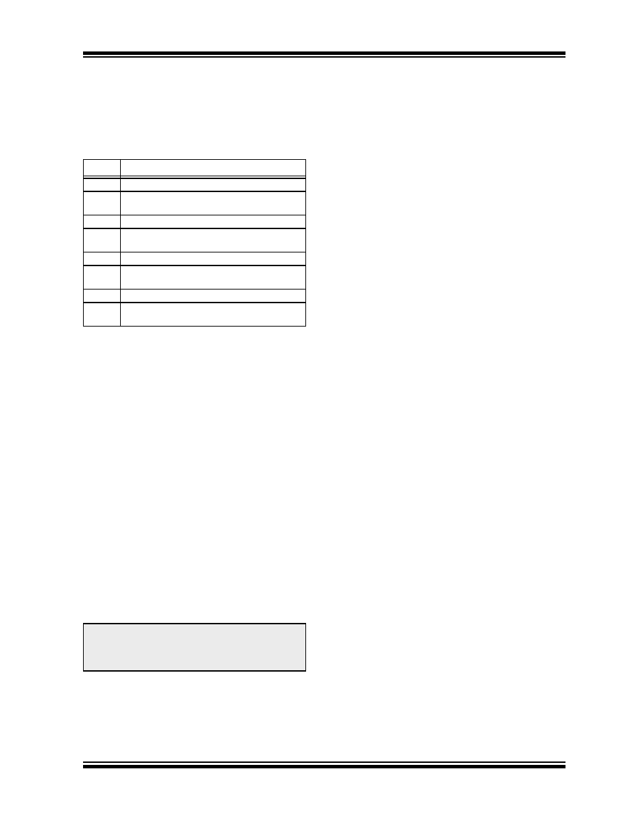
TABLE 15-1:
DEAD-TIME SELECTION BITS
15.7.3
DEAD-TIME RANGES
The amount of dead time provided by each dead-time
unit is selected by specifying the input clock prescaler
value and a 6-bit unsigned value. The amount of dead
time provided by each unit may be set independently.
Four input clock prescaler selections have been pro-
vided to allow a suitable range of dead times, based on
the device operating frequency. The clock prescaler
option may be selected independently for each of the
two dead-time values. The dead-time clock prescaler
values are selected using the DTAPS<1:0> and
DTBPS<1:0> control bits in the DTCON1 SFR. One of
four clock prescaler options (TCY, 2 TCY, 4 TCY or 8 TCY)
may be selected for each of the dead-time values.
After the prescaler values are selected, the dead time
for each unit is adjusted by loading two 6-bit unsigned
values into the DTCON1 SFR.
The dead-time unit prescalers are cleared on the
following events:
On a load of the down timer due to a duty cycle
comparison edge event.
On a write to the DTCON1 or DTCON2 registers.
On any device Reset.
15.8
Independent PWM Output
An Independent PWM Output mode is required for
driving certain types of loads. A particular PWM output
pair is in the Independent Output mode when the cor-
responding PMODx bit in the PWMCON1 register is
set. No dead-time control is implemented between
adjacent PWM I/O pins when the module is operating
in the Independent PWM Output mode and both I/O
pins are allowed to be active simultaneously.
In the Independent PWM Output mode, each duty cycle
generator is connected to both of the PWM I/O pins in
an output pair. By using the associated Duty Cycle reg-
ister and the appropriate bits in the OVDCON register,
the user may select the following signal output options
for each PWM I/O pin operating in this mode:
I/O pin outputs PWM signal
I/O pin inactive
I/O pin active
15.9
Single Pulse PWM Operation
The PWM module produces single pulse outputs when
the PTCON control bits PTMOD<1:0> = 10. Only edge-
aligned outputs may be produced in the Single Pulse
mode. In Single Pulse mode, the PWM I/O pin(s) are
driven to the active state when the PTEN bit is set.
When a match with a Duty Cycle register occurs, the
PWM I/O pin is driven to the inactive state. When a
match with the PTPER register occurs, the PTMR
register is cleared, all active PWM I/O pins are driven
to the inactive state, the PTEN bit is cleared and an
interrupt is generated.
15.10 PWM Output Override
The PWM output override bits allow the user to manu-
ally drive the PWM I/O pins to specified logic states,
independent of the duty cycle comparison units.
All control bits associated with the PWM output over-
ride function are contained in the OVDCON register.
The upper half of the OVDCON register contains eight
bits, POVDxH<4:1> and POVDxL<4:1>, that determine
which PWM I/O pins will be overridden. The lower half
of
the
OVDCON
register
contains
eight
bits,
POUTxH<4:1> and POUTxL<4:1>, that determine the
state of the PWM I/O pins when a particular output is
overridden via the POVD bits.
15.10.1
COMPLEMENTARY OUTPUT MODE
When a PWMxL pin is driven active via the OVDCON
register, the output signal is forced to be the comple-
ment of the corresponding PWMxH pin in the pair.
Dead-time insertion is still performed when PWM
channels are overridden manually.
Bit
Function
DTS1A
Selects PWM1L/PWM1H active edge dead time.
DTS1I
Selects PWM1L/PWM1H inactive edge
dead time.
DTS2A
Selects PWM2L/PWM2H active edge dead time.
DTS2I
Selects PWM2L/PWM2H inactive edge
dead time.
DTS3A
Selects PWM3L/PWM3H active edge dead time.
DTS3I
Selects PWM3L/PWM3H inactive edge
dead time.
DTS4A
Selects PWM4L/PWM4H active edge dead time.
DTS4I
Selects PWM4L/PWM4H inactive edge
dead time.
Note:
The user should not modify the DTCON1
or DTCON2 values while the PWM mod-
ule is operating (PTEN = 1). Unexpected
results may occur.
相关PDF资料 |
PDF描述 |
|---|---|
| PIC16LC712-04/P | IC MCU OTP 1KX14 A/D PWM 18DIP |
| PIC18F24K22T-I/ML | IC MCU 8BIT 16KB FLASH 28QFN |
| PIC18LF24K22T-I/ML | IC MCU 8BIT 16KB FLASH 28QFN |
| PIC16LF1938-E/ML | MCU 8BIT 16K FLASH 28QFN |
| PIC16F1938-E/MV | MCU 8BIT 16K FLASH 28UQFN |
相关代理商/技术参数 |
参数描述 |
|---|---|
| PIC18F45K22-E/ML | 功能描述:8位微控制器 -MCU 32KB Flash 1536B RAM 8B nanoWatt RoHS:否 制造商:Silicon Labs 核心:8051 处理器系列:C8051F39x 数据总线宽度:8 bit 最大时钟频率:50 MHz 程序存储器大小:16 KB 数据 RAM 大小:1 KB 片上 ADC:Yes 工作电源电压:1.8 V to 3.6 V 工作温度范围:- 40 C to + 105 C 封装 / 箱体:QFN-20 安装风格:SMD/SMT |
| PIC18F45K22-E/MV | 功能描述:8位微控制器 -MCU 32KB 1536b RAM 8bit familynanoWatt XLP RoHS:否 制造商:Silicon Labs 核心:8051 处理器系列:C8051F39x 数据总线宽度:8 bit 最大时钟频率:50 MHz 程序存储器大小:16 KB 数据 RAM 大小:1 KB 片上 ADC:Yes 工作电源电压:1.8 V to 3.6 V 工作温度范围:- 40 C to + 105 C 封装 / 箱体:QFN-20 安装风格:SMD/SMT |
| PIC18F45K22-E/P | 功能描述:8位微控制器 -MCU 32KB 1536bytes-RAM 8B nanoWatt RoHS:否 制造商:Silicon Labs 核心:8051 处理器系列:C8051F39x 数据总线宽度:8 bit 最大时钟频率:50 MHz 程序存储器大小:16 KB 数据 RAM 大小:1 KB 片上 ADC:Yes 工作电源电压:1.8 V to 3.6 V 工作温度范围:- 40 C to + 105 C 封装 / 箱体:QFN-20 安装风格:SMD/SMT |
| PIC18F45K22-E/PT | 功能描述:8位微控制器 -MCU 32KB Flash 1536B RAM 8B nanoWatt RoHS:否 制造商:Silicon Labs 核心:8051 处理器系列:C8051F39x 数据总线宽度:8 bit 最大时钟频率:50 MHz 程序存储器大小:16 KB 数据 RAM 大小:1 KB 片上 ADC:Yes 工作电源电压:1.8 V to 3.6 V 工作温度范围:- 40 C to + 105 C 封装 / 箱体:QFN-20 安装风格:SMD/SMT |
| PIC18F45K22-I/ML | 功能描述:8位微控制器 -MCU 32KB Flash 1536B RAM 8B nanoWatt RoHS:否 制造商:Silicon Labs 核心:8051 处理器系列:C8051F39x 数据总线宽度:8 bit 最大时钟频率:50 MHz 程序存储器大小:16 KB 数据 RAM 大小:1 KB 片上 ADC:Yes 工作电源电压:1.8 V to 3.6 V 工作温度范围:- 40 C to + 105 C 封装 / 箱体:QFN-20 安装风格:SMD/SMT |
发布紧急采购,3分钟左右您将得到回复。