参数资料
| 型号: | PIC18F4610-E/ML |
| 厂商: | Microchip Technology |
| 文件页数: | 36/234页 |
| 文件大小: | 0K |
| 描述: | IC MCU FLASH 32KX16 44QFN |
| 标准包装: | 45 |
| 系列: | PIC® 18F |
| 核心处理器: | PIC |
| 芯体尺寸: | 8-位 |
| 速度: | 25MHz |
| 连通性: | I²C,SPI,UART/USART |
| 外围设备: | 欠压检测/复位,HLVD,POR,PWM,WDT |
| 输入/输出数: | 36 |
| 程序存储器容量: | 64KB(32K x 16) |
| 程序存储器类型: | 闪存 |
| RAM 容量: | 3.8K x 8 |
| 电压 - 电源 (Vcc/Vdd): | 4.2 V ~ 5.5 V |
| 数据转换器: | A/D 13x10b |
| 振荡器型: | 内部 |
| 工作温度: | -40°C ~ 125°C |
| 封装/外壳: | 44-VQFN 裸露焊盘 |
| 包装: | 管件 |
第1页第2页第3页第4页第5页第6页第7页第8页第9页第10页第11页第12页第13页第14页第15页第16页第17页第18页第19页第20页第21页第22页第23页第24页第25页第26页第27页第28页第29页第30页第31页第32页第33页第34页第35页当前第36页第37页第38页第39页第40页第41页第42页第43页第44页第45页第46页第47页第48页第49页第50页第51页第52页第53页第54页第55页第56页第57页第58页第59页第60页第61页第62页第63页第64页第65页第66页第67页第68页第69页第70页第71页第72页第73页第74页第75页第76页第77页第78页第79页第80页第81页第82页第83页第84页第85页第86页第87页第88页第89页第90页第91页第92页第93页第94页第95页第96页第97页第98页第99页第100页第101页第102页第103页第104页第105页第106页第107页第108页第109页第110页第111页第112页第113页第114页第115页第116页第117页第118页第119页第120页第121页第122页第123页第124页第125页第126页第127页第128页第129页第130页第131页第132页第133页第134页第135页第136页第137页第138页第139页第140页第141页第142页第143页第144页第145页第146页第147页第148页第149页第150页第151页第152页第153页第154页第155页第156页第157页第158页第159页第160页第161页第162页第163页第164页第165页第166页第167页第168页第169页第170页第171页第172页第173页第174页第175页第176页第177页第178页第179页第180页第181页第182页第183页第184页第185页第186页第187页第188页第189页第190页第191页第192页第193页第194页第195页第196页第197页第198页第199页第200页第201页第202页第203页第204页第205页第206页第207页第208页第209页第210页第211页第212页第213页第214页第215页第216页第217页第218页第219页第220页第221页第222页第223页第224页第225页第226页第227页第228页第229页第230页第231页第232页第233页第234页
PIC18F2X1X/4X1X
DS39636D-page 132
2009 Microchip Technology Inc.
14.1
CCP Module Configuration
Each Capture/Compare/PWM module is associated
with a control register (generically, CCPxCON) and a
data register (CCPRx). The data register, in turn, is
comprised of two 8-bit registers: CCPRxL (low byte)
and CCPRxH (high byte). All registers are both
readable and writable.
14.1.1
CCP MODULES AND TIMER
RESOURCES
The CCP modules utilize Timers 1, 2 or 3, depending
on the mode selected. Timer1 and Timer3 are available
to modules in Capture or Compare modes, while
Timer2 is available for modules in PWM mode.
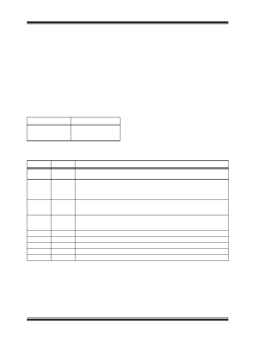
TABLE 14-1:
CCP MODE – TIMER
RESOURCE
The assignment of a particular timer to a module is
determined by the Timer-to-CCP enable bits in the
T3CON register (Register 13-1). Both modules may be
active at any given time and may share the same timer
resource if they are configured to operate in the same
mode (Capture/Compare or PWM) at the same time. The
interactions between the two modules are summarized in
Figure 14-1 and Figure 14-2. In Timer1 in Asynchronous
Counter mode, the capture operation will not work.
14.1.2
CCP2 PIN ASSIGNMENT
The pin assignment for CCP2 (Capture input, Compare
and PWM output) can change, based on device config-
uration. The CCP2MX Configuration bit determines
which pin CCP2 is multiplexed to. By default, it is
assigned to RC1 (CCP2MX = 1). If the Configuration bit
is cleared, CCP2 is multiplexed with RB3.
Changing the pin assignment of CCP2 does not auto-
matically change any requirements for configuring the
port pin. Users must always verify that the appropriate
TRIS register is configured correctly for CCP2
operation, regardless of where it is located.
TABLE 14-2:
INTERACTIONS BETWEEN CCP1 AND CCP2 FOR TIMER RESOURCES
CCP/ECCP Mode
Timer Resource
Capture
Compare
PWM
Timer1 or Timer3
Timer2
CCP1 Mode CCP2 Mode
Interaction
Capture
Each module can use TMR1 or TMR3 as the time base. The time base can be different
for each CCP.
Capture
Compare
CCP2 can be configured for the special event trigger to reset TMR1 or TMR3
(depending upon which time base is used). Automatic A/D conversions on trigger event
can also be done. Operation of CCP1 could be affected if it is using the same timer as a
time base.
Compare
Capture
CCP1 can be configured for the special event trigger to reset TMR1 or TMR3 (depending
upon which time base is used). Operation of CCP2 could be affected if it is using the
same timer as a time base.
Compare
Either module can be configured for the Special Event Trigger to reset the time base.
Automatic A/D conversions on CCP2 trigger event can be done. Conflicts may occur if
both modules are using the same time base.
Capture
PWM(1)
None
Compare
PWM(1)
None
PWM(1)
Capture
None
PWM(1)
Compare
None
PWM(1)
PWM
Both PWMs will have the same frequency and update rate (TMR2 interrupt).
Note 1:
Includes standard and Enhanced PWM operation.
相关PDF资料 |
PDF描述 |
|---|---|
| PIC18LF2331T-I/SO | IC MCU FLASH 4KX16 28SOIC |
| PIC18F4515T-I/PT | IC MCU FLASH 24KX16 44TQFP |
| PIC18F4431T-I/ML | IC MCU FLASH 8KX16 44QFN |
| PIC18F4431-E/ML | IC MCU FLASH 8KX16 44QFN |
| PIC18F4410T-I/ML | IC MCU FLASH 8KX16 44QFN |
相关代理商/技术参数 |
参数描述 |
|---|---|
| PIC18F4610-I/ML | 功能描述:8位微控制器 -MCU 64KB 3968 RAM 36 I/O RoHS:否 制造商:Silicon Labs 核心:8051 处理器系列:C8051F39x 数据总线宽度:8 bit 最大时钟频率:50 MHz 程序存储器大小:16 KB 数据 RAM 大小:1 KB 片上 ADC:Yes 工作电源电压:1.8 V to 3.6 V 工作温度范围:- 40 C to + 105 C 封装 / 箱体:QFN-20 安装风格:SMD/SMT |
| PIC18F4610-I/P | 功能描述:8位微控制器 -MCU 64KB 3968 RAM 36 I/O RoHS:否 制造商:Silicon Labs 核心:8051 处理器系列:C8051F39x 数据总线宽度:8 bit 最大时钟频率:50 MHz 程序存储器大小:16 KB 数据 RAM 大小:1 KB 片上 ADC:Yes 工作电源电压:1.8 V to 3.6 V 工作温度范围:- 40 C to + 105 C 封装 / 箱体:QFN-20 安装风格:SMD/SMT |
| PIC18F4610-I/P | 制造商:Microchip Technology Inc 功能描述:8-Bit Microcontroller IC |
| PIC18F4610-I/PT | 功能描述:8位微控制器 -MCU 64KB 3968 RAM 36 I/O RoHS:否 制造商:Silicon Labs 核心:8051 处理器系列:C8051F39x 数据总线宽度:8 bit 最大时钟频率:50 MHz 程序存储器大小:16 KB 数据 RAM 大小:1 KB 片上 ADC:Yes 工作电源电压:1.8 V to 3.6 V 工作温度范围:- 40 C to + 105 C 封装 / 箱体:QFN-20 安装风格:SMD/SMT |
| PIC18F4610T-I/ML | 功能描述:8位微控制器 -MCU 64KB 3968 RAM 36 I/O RoHS:否 制造商:Silicon Labs 核心:8051 处理器系列:C8051F39x 数据总线宽度:8 bit 最大时钟频率:50 MHz 程序存储器大小:16 KB 数据 RAM 大小:1 KB 片上 ADC:Yes 工作电源电压:1.8 V to 3.6 V 工作温度范围:- 40 C to + 105 C 封装 / 箱体:QFN-20 安装风格:SMD/SMT |
发布紧急采购,3分钟左右您将得到回复。