- 您现在的位置:买卖IC网 > PDF目录11421 > PIC18F6410-E/PT (Microchip Technology)IC PIC MCU FLASH 16KX16 64TQFP PDF资料下载
参数资料
| 型号: | PIC18F6410-E/PT |
| 厂商: | Microchip Technology |
| 文件页数: | 6/411页 |
| 文件大小: | 0K |
| 描述: | IC PIC MCU FLASH 16KX16 64TQFP |
| 产品培训模块: | Asynchronous Stimulus PIC18 J Series MCU Overview |
| 标准包装: | 160 |
| 系列: | PIC® 18F |
| 核心处理器: | PIC |
| 芯体尺寸: | 8-位 |
| 速度: | 25MHz |
| 连通性: | I²C,SPI,UART/USART |
| 外围设备: | 欠压检测/复位,HLVD,POR,PWM,WDT |
| 输入/输出数: | 54 |
| 程序存储器容量: | 16KB(8K x 16) |
| 程序存储器类型: | 闪存 |
| RAM 容量: | 768 x 8 |
| 电压 - 电源 (Vcc/Vdd): | 4.2 V ~ 5.5 V |
| 数据转换器: | A/D 12x10b |
| 振荡器型: | 内部 |
| 工作温度: | -40°C ~ 125°C |
| 封装/外壳: | 64-TQFP |
| 包装: | 托盘 |
第1页第2页第3页第4页第5页当前第6页第7页第8页第9页第10页第11页第12页第13页第14页第15页第16页第17页第18页第19页第20页第21页第22页第23页第24页第25页第26页第27页第28页第29页第30页第31页第32页第33页第34页第35页第36页第37页第38页第39页第40页第41页第42页第43页第44页第45页第46页第47页第48页第49页第50页第51页第52页第53页第54页第55页第56页第57页第58页第59页第60页第61页第62页第63页第64页第65页第66页第67页第68页第69页第70页第71页第72页第73页第74页第75页第76页第77页第78页第79页第80页第81页第82页第83页第84页第85页第86页第87页第88页第89页第90页第91页第92页第93页第94页第95页第96页第97页第98页第99页第100页第101页第102页第103页第104页第105页第106页第107页第108页第109页第110页第111页第112页第113页第114页第115页第116页第117页第118页第119页第120页第121页第122页第123页第124页第125页第126页第127页第128页第129页第130页第131页第132页第133页第134页第135页第136页第137页第138页第139页第140页第141页第142页第143页第144页第145页第146页第147页第148页第149页第150页第151页第152页第153页第154页第155页第156页第157页第158页第159页第160页第161页第162页第163页第164页第165页第166页第167页第168页第169页第170页第171页第172页第173页第174页第175页第176页第177页第178页第179页第180页第181页第182页第183页第184页第185页第186页第187页第188页第189页第190页第191页第192页第193页第194页第195页第196页第197页第198页第199页第200页第201页第202页第203页第204页第205页第206页第207页第208页第209页第210页第211页第212页第213页第214页第215页第216页第217页第218页第219页第220页第221页第222页第223页第224页第225页第226页第227页第228页第229页第230页第231页第232页第233页第234页第235页第236页第237页第238页第239页第240页第241页第242页第243页第244页第245页第246页第247页第248页第249页第250页第251页第252页第253页第254页第255页第256页第257页第258页第259页第260页第261页第262页第263页第264页第265页第266页第267页第268页第269页第270页第271页第272页第273页第274页第275页第276页第277页第278页第279页第280页第281页第282页第283页第284页第285页第286页第287页第288页第289页第290页第291页第292页第293页第294页第295页第296页第297页第298页第299页第300页第301页第302页第303页第304页第305页第306页第307页第308页第309页第310页第311页第312页第313页第314页第315页第316页第317页第318页第319页第320页第321页第322页第323页第324页第325页第326页第327页第328页第329页第330页第331页第332页第333页第334页第335页第336页第337页第338页第339页第340页第341页第342页第343页第344页第345页第346页第347页第348页第349页第350页第351页第352页第353页第354页第355页第356页第357页第358页第359页第360页第361页第362页第363页第364页第365页第366页第367页第368页第369页第370页第371页第372页第373页第374页第375页第376页第377页第378页第379页第380页第381页第382页第383页第384页第385页第386页第387页第388页第389页第390页第391页第392页第393页第394页第395页第396页第397页第398页第399页第400页第401页第402页第403页第404页第405页第406页第407页第408页第409页第410页第411页
2010-2012 Microchip Technology Inc.
DS39977F-page 103
PIC18F66K80 FAMILY
6.1.2
PROGRAM COUNTER
The Program Counter (PC) specifies the address of the
instruction to fetch for execution. The PC is 21 bits wide
and contained in three separate 8-bit registers.
The low byte, known as the PCL register, is both
readable and writable. The high byte, or PCH register,
contains the PC<15:8> bits and is not directly readable
or writable. Updates to the PCH register are performed
through the PCLATH register. The upper byte is called
PCU. This register contains the PC<20:16> bits; it is also
not directly readable or writable. Updates to the PCU
register are performed through the PCLATU register.
The contents of PCLATH and PCLATU are transferred to
the Program Counter by any operation that writes PCL.
Similarly, the upper two bytes of the Program Counter
are transferred to PCLATH and PCLATU by an operation
that reads PCL. This is useful for computed offsets to the
PC (see Section 6.1.5.1 “Computed GOTO”).
The PC addresses bytes in the program memory. To
prevent the PC from becoming misaligned with word
instructions, the Least Significant bit (LSb) of PCL is
fixed to a value of ‘0’. The PC increments by two to
address sequential instructions in the program memory.
The CALL, RCALL, GOTO and program branch
instructions write to the Program Counter directly. For
these instructions, the contents of PCLATH and
PCLATU are not transferred to the Program Counter.
6.1.3
RETURN ADDRESS STACK
The return address stack enables execution of any
combination of up to 31 program calls and interrupts.
The PC is pushed onto the stack when a CALL or
RCALL
instruction is executed or an interrupt is
Acknowledged. The PC value is pulled off the stack on
a RETURN, RETLW or a RETFIE instruction. The value
is also pulled off the stack on ADDULNK and SUBULNK
instructions if the extended instruction set is enabled.
PCLATU and PCLATH are not affected by any of the
RETURN
or CALL instructions.
The stack operates as a 31-word by 21-bit RAM and a
5-bit Stack Pointer, STKPTR. The stack space is not
part of either program or data space. The Stack Pointer
is readable and writable and the address on the top of
the stack is readable and writable through the
Top-of-Stack (TOS) Special Function Registers. Data
can also be pushed to, or popped from the stack, using
these registers.
A CALL type instruction causes a push onto the stack.
The Stack Pointer is first incremented and the location
pointed to by the Stack Pointer is written with the
contents of the PC (already pointing to the instruction
following the CALL). A RETURN type instruction causes
a pop from the stack. The contents of the location
pointed to by the STKPTR are transferred to the PC
and then the Stack Pointer is decremented.
The Stack Pointer is initialized to ‘00000’ after all
Resets. There is no RAM associated with the location
corresponding to a Stack Pointer value of ‘00000’; this
is only a Reset value. Status bits indicate if the stack is
full, has overflowed or has underflowed.
6.1.3.1
Top-of-Stack Access
Only the top of the return address stack is readable and
writable. A set of three registers, TOSU:TOSH:TOSL,
holds the contents of the stack location pointed to by
the STKPTR register (Figure 6-3). This allows users to
implement a software stack, if necessary. After a CALL,
RCALL
or interrupt (or ADDULNK and SUBULNK instruc-
tions, if the extended instruction set is enabled), the
software can read the pushed value by reading the
TOSU:TOSH:TOSL registers. These values can be
placed on a user-defined software stack. At return time,
the
software
can
return
these
values
to
TOSU:TOSH:TOSL and do a return.
While accessing the stack, users must disable the
Global Interrupt Enable bits to prevent inadvertent
stack corruption.
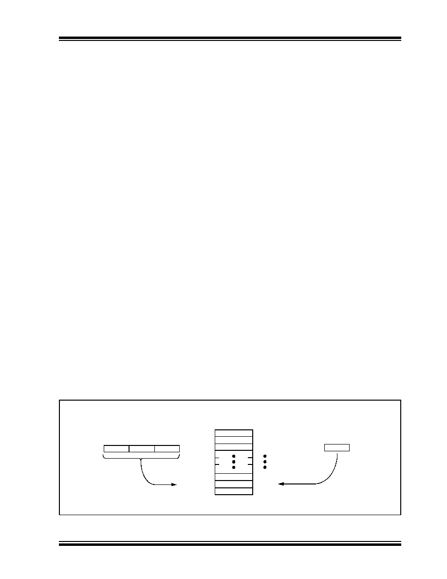
FIGURE 6-3:
RETURN ADDRESS STACK AND ASSOCIATED REGISTERS
00011
001A34h
11111
11110
11101
00010
00001
00000
00010
Return Address Stack<20:0>
Top-of-Stack
000D58h
TOSL
TOSH
TOSU
34h
1Ah
00h
STKPTR<4:0>
Top-of-Stack Registers
Stack Pointer
相关PDF资料 |
PDF描述 |
|---|---|
| DG409DVZ | IC MULTIPLEXER DUAL 4X1 16TSSOP |
| VE-B3X-IY | CONVERTER MOD DC/DC 5.2V 50W |
| VI-23H-CV-F4 | CONVERTER MOD DC/DC 52V 150W |
| PIC16LC620-04I/SO | IC MCU OTP 512X14 COMP 18SOIC |
| PIC24HJ32GP302-E/MM | IC PIC MCU FLASH 32K 28-QFN |
相关代理商/技术参数 |
参数描述 |
|---|---|
| PIC18F6410-I/PT | 功能描述:8位微控制器 -MCU 16kBF 768RM 68I/O RoHS:否 制造商:Silicon Labs 核心:8051 处理器系列:C8051F39x 数据总线宽度:8 bit 最大时钟频率:50 MHz 程序存储器大小:16 KB 数据 RAM 大小:1 KB 片上 ADC:Yes 工作电源电压:1.8 V to 3.6 V 工作温度范围:- 40 C to + 105 C 封装 / 箱体:QFN-20 安装风格:SMD/SMT |
| PIC18F6410-I/PT | 制造商:Microchip Technology Inc 功能描述:IC 8BIT FLASH MCU 18F6410 TQFP64 |
| PIC18F6410T-I/PT | 功能描述:8位微控制器 -MCU 16kBF 768RM 68I/O RoHS:否 制造商:Silicon Labs 核心:8051 处理器系列:C8051F39x 数据总线宽度:8 bit 最大时钟频率:50 MHz 程序存储器大小:16 KB 数据 RAM 大小:1 KB 片上 ADC:Yes 工作电源电压:1.8 V to 3.6 V 工作温度范围:- 40 C to + 105 C 封装 / 箱体:QFN-20 安装风格:SMD/SMT |
| PIC18F6490-E/PT | 功能描述:8位微控制器 -MCU 16kBF 768RM 68I/O RoHS:否 制造商:Silicon Labs 核心:8051 处理器系列:C8051F39x 数据总线宽度:8 bit 最大时钟频率:50 MHz 程序存储器大小:16 KB 数据 RAM 大小:1 KB 片上 ADC:Yes 工作电源电压:1.8 V to 3.6 V 工作温度范围:- 40 C to + 105 C 封装 / 箱体:QFN-20 安装风格:SMD/SMT |
| PIC18F6490-I/PT | 功能描述:8位微控制器 -MCU 16kBF 768RM 68I/O RoHS:否 制造商:Silicon Labs 核心:8051 处理器系列:C8051F39x 数据总线宽度:8 bit 最大时钟频率:50 MHz 程序存储器大小:16 KB 数据 RAM 大小:1 KB 片上 ADC:Yes 工作电源电压:1.8 V to 3.6 V 工作温度范围:- 40 C to + 105 C 封装 / 箱体:QFN-20 安装风格:SMD/SMT |
发布紧急采购,3分钟左右您将得到回复。