- 您现在的位置:买卖IC网 > PDF目录11283 > PIC18F6520T-E/PT (Microchip Technology)IC PIC MCU FLASH 16KX16 64TQFP PDF资料下载
参数资料
| 型号: | PIC18F6520T-E/PT |
| 厂商: | Microchip Technology |
| 文件页数: | 139/165页 |
| 文件大小: | 0K |
| 描述: | IC PIC MCU FLASH 16KX16 64TQFP |
| 产品培训模块: | Asynchronous Stimulus |
| 标准包装: | 1,200 |
| 系列: | PIC® 18F |
| 核心处理器: | PIC |
| 芯体尺寸: | 8-位 |
| 速度: | 25MHz |
| 连通性: | I²C,SPI,UART/USART |
| 外围设备: | 欠压检测/复位,LVD,POR,PWM,WDT |
| 输入/输出数: | 52 |
| 程序存储器容量: | 32KB(16K x 16) |
| 程序存储器类型: | 闪存 |
| EEPROM 大小: | 1K x 8 |
| RAM 容量: | 2K x 8 |
| 电压 - 电源 (Vcc/Vdd): | 4.2 V ~ 5.5 V |
| 数据转换器: | A/D 12x10b |
| 振荡器型: | 内部 |
| 工作温度: | -40°C ~ 125°C |
| 封装/外壳: | 64-TQFP |
| 包装: | 带卷 (TR) |
第1页第2页第3页第4页第5页第6页第7页第8页第9页第10页第11页第12页第13页第14页第15页第16页第17页第18页第19页第20页第21页第22页第23页第24页第25页第26页第27页第28页第29页第30页第31页第32页第33页第34页第35页第36页第37页第38页第39页第40页第41页第42页第43页第44页第45页第46页第47页第48页第49页第50页第51页第52页第53页第54页第55页第56页第57页第58页第59页第60页第61页第62页第63页第64页第65页第66页第67页第68页第69页第70页第71页第72页第73页第74页第75页第76页第77页第78页第79页第80页第81页第82页第83页第84页第85页第86页第87页第88页第89页第90页第91页第92页第93页第94页第95页第96页第97页第98页第99页第100页第101页第102页第103页第104页第105页第106页第107页第108页第109页第110页第111页第112页第113页第114页第115页第116页第117页第118页第119页第120页第121页第122页第123页第124页第125页第126页第127页第128页第129页第130页第131页第132页第133页第134页第135页第136页第137页第138页当前第139页第140页第141页第142页第143页第144页第145页第146页第147页第148页第149页第150页第151页第152页第153页第154页第155页第156页第157页第158页第159页第160页第161页第162页第163页第164页第165页
2004 Microchip Technology Inc.
DS39609B-page 73
PIC18F6520/8520/6620/8620/6720/8720
6.2
16-bit Mode
The External
Memory Interface implemented
in
PIC18F8X20 devices operates only in 16-bit mode.
The mode selection is not software configurable, but is
programmed via the configuration bits.
The WM<1:0> bits in the MEMCON register determine
three types of connections in 16-bit mode. They are
referred to as:
16-bit Byte Write
16-bit Word Write
16-bit Byte Select
These three different configurations allow the designer
maximum flexibility in using 8-bit and 16-bit memory
devices.
For all 16-bit modes, the Address Latch Enable (ALE)
pin indicates that the address bits A<15:0> are
available on the External Memory Interface bus.
Following the address latch, the Output Enable signal
(OE) will enable both bytes of program memory at once
to form a 16-bit instruction word. The Chip Enable
signal (CE) is active at any time that the microcontroller
accesses external memory, whether reading or writing;
it is inactive (asserted high) whenever the device is in
Sleep mode.
In Byte Select mode, JEDEC standard Flash memories
will require BA0 for the byte address line and one I/O
line to select between Byte and Word mode. The other
16-bit modes do not need BA0. JEDEC standard static
RAM memories will use the UB or LB signals for byte
selection.
6.2.1
16-BIT BYTE WRITE MODE
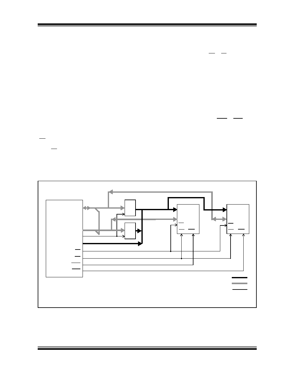
Figure 6-1 shows an example of 16-bit Byte Write
mode for PIC18F8X20 devices. This mode is used for
two separate 8-bit memories connected for 16-bit oper-
ation. This generally includes basic EPROM and Flash
devices. It allows table writes to byte-wide external
memories.
During a TBLWT instruction cycle, the TABLAT data is
presented on the upper and lower bytes of the
AD15:AD0 bus. The appropriate WRH or WRL control
line is strobed on the LSb of the TBLPTR.
FIGURE 6-1:
16-BIT BYTE WRITE MODE EXAMPLE
AD<7:0>
A<19:16>
ALE
D<15:8>
373
A<x:0>
D<7:0>
A<19:0>
A<x:0>
D<7:0>
373
OE
WRH
OE
WR(1)
CE
Note 1:
This signal only applies to table writes. See Section 5.1 “Table Reads and Table Writes”.
WRL
D<7:0>
(LSB)
(MSB)
PIC18F8X20
D<7:0>
AD<15:8>
Address Bus
Data Bus
Control Lines
CE
相关PDF资料 |
PDF描述 |
|---|---|
| PIC24FJ128GB206-I/PT | MCU PIC 16BIT FLASH USB 64TQFP |
| PIC18LF4685T-I/ML | IC PIC MCU FLASH 48KX16 44QFN |
| PIC18F458-E/P | IC MCU FLASH 16KX16 W/CAN 40 DIP |
| PIC16LC774/P | IC MCU OTP 4KX14 A/D PWM 40DIP |
| PIC16F877T-20/PT | IC MCU FLASH 8KX14 EE 44TQFP |
相关代理商/技术参数 |
参数描述 |
|---|---|
| PIC18F6520T-I/PT | 功能描述:8位微控制器 -MCU 32KB 2048 RAM 52I/O RoHS:否 制造商:Silicon Labs 核心:8051 处理器系列:C8051F39x 数据总线宽度:8 bit 最大时钟频率:50 MHz 程序存储器大小:16 KB 数据 RAM 大小:1 KB 片上 ADC:Yes 工作电源电压:1.8 V to 3.6 V 工作温度范围:- 40 C to + 105 C 封装 / 箱体:QFN-20 安装风格:SMD/SMT |
| PIC18F6520T-I/PTG | 功能描述:8位微控制器 -MCU 32KB 2048 RAM 52I/O Lead Free Package RoHS:否 制造商:Silicon Labs 核心:8051 处理器系列:C8051F39x 数据总线宽度:8 bit 最大时钟频率:50 MHz 程序存储器大小:16 KB 数据 RAM 大小:1 KB 片上 ADC:Yes 工作电源电压:1.8 V to 3.6 V 工作温度范围:- 40 C to + 105 C 封装 / 箱体:QFN-20 安装风格:SMD/SMT |
| PIC18F6525-E/PT | 功能描述:8位微控制器 -MCU 48KB 3840 RAM 52I/O RoHS:否 制造商:Silicon Labs 核心:8051 处理器系列:C8051F39x 数据总线宽度:8 bit 最大时钟频率:50 MHz 程序存储器大小:16 KB 数据 RAM 大小:1 KB 片上 ADC:Yes 工作电源电压:1.8 V to 3.6 V 工作温度范围:- 40 C to + 105 C 封装 / 箱体:QFN-20 安装风格:SMD/SMT |
| PIC18F6525-I/PT | 功能描述:8位微控制器 -MCU 48KB 3840 RAM 52I/O RoHS:否 制造商:Silicon Labs 核心:8051 处理器系列:C8051F39x 数据总线宽度:8 bit 最大时钟频率:50 MHz 程序存储器大小:16 KB 数据 RAM 大小:1 KB 片上 ADC:Yes 工作电源电压:1.8 V to 3.6 V 工作温度范围:- 40 C to + 105 C 封装 / 箱体:QFN-20 安装风格:SMD/SMT |
| PIC18F6525-I/PT | 制造商:Microchip Technology Inc 功能描述:IC 8BIT FLASH MCU 18F6525 TQFP64 |
发布紧急采购,3分钟左右您将得到回复。