- 您现在的位置:买卖IC网 > PDF目录3847 > PIC18F66J55-I/PT (Microchip Technology)IC PIC MCU FLASH 48KX16 64TQFP PDF资料下载
参数资料
| 型号: | PIC18F66J55-I/PT |
| 厂商: | Microchip Technology |
| 文件页数: | 31/61页 |
| 文件大小: | 0K |
| 描述: | IC PIC MCU FLASH 48KX16 64TQFP |
| 产品培训模块: | Asynchronous Stimulus PIC18 J Series MCU Overview 8-bit PIC® Microcontroller Portfolio |
| 标准包装: | 160 |
| 系列: | PIC® 18F |
| 核心处理器: | PIC |
| 芯体尺寸: | 8-位 |
| 速度: | 48MHz |
| 连通性: | I²C,SPI,UART/USART,USB |
| 外围设备: | 欠压检测/复位,LVD,POR,PWM,WDT |
| 输入/输出数: | 49 |
| 程序存储器容量: | 96KB(48K x 16) |
| 程序存储器类型: | 闪存 |
| RAM 容量: | 3.8K x 8 |
| 电压 - 电源 (Vcc/Vdd): | 2 V ~ 3.6 V |
| 数据转换器: | A/D 8x10b |
| 振荡器型: | 内部 |
| 工作温度: | -40°C ~ 85°C |
| 封装/外壳: | 64-TQFP |
| 包装: | 托盘 |
| 产品目录页面: | 644 (CN2011-ZH PDF) |
| 配用: | AC162087-ND - HEADER MPLAB ICD2 18F87J50 68/84 MA180021-ND - MODULE PLUG-IN 18F87J50 FS USB AC164327-ND - MODULE SKT FOR 64TQFP |
第1页第2页第3页第4页第5页第6页第7页第8页第9页第10页第11页第12页第13页第14页第15页第16页第17页第18页第19页第20页第21页第22页第23页第24页第25页第26页第27页第28页第29页第30页当前第31页第32页第33页第34页第35页第36页第37页第38页第39页第40页第41页第42页第43页第44页第45页第46页第47页第48页第49页第50页第51页第52页第53页第54页第55页第56页第57页第58页第59页第60页第61页
Philips Semiconductors
Product data
P87LPC767
Low power, low price, low pin count (20 pin)
microcontroller with 4-kbyte OTP and 8-bit A/D converter
2002 Mar 25
34
SU01176
TL0
(8 BITS)
OSC/6
OR
OSC/12
OVERFLOW
T0 PIN
T0OE
TOGGLE
CONTROL
C/T = 1
C/T = 0
T0 PIN
TR0
GATE
INT0 PIN
INTERRUPT
TF0
TH0
(8 BITS)
OVERFLOW
T1 PIN
T1OE
TOGGLE
CONTROL
INTERRUPT
TF1
TR1
OSC/6
OR
OSC/12
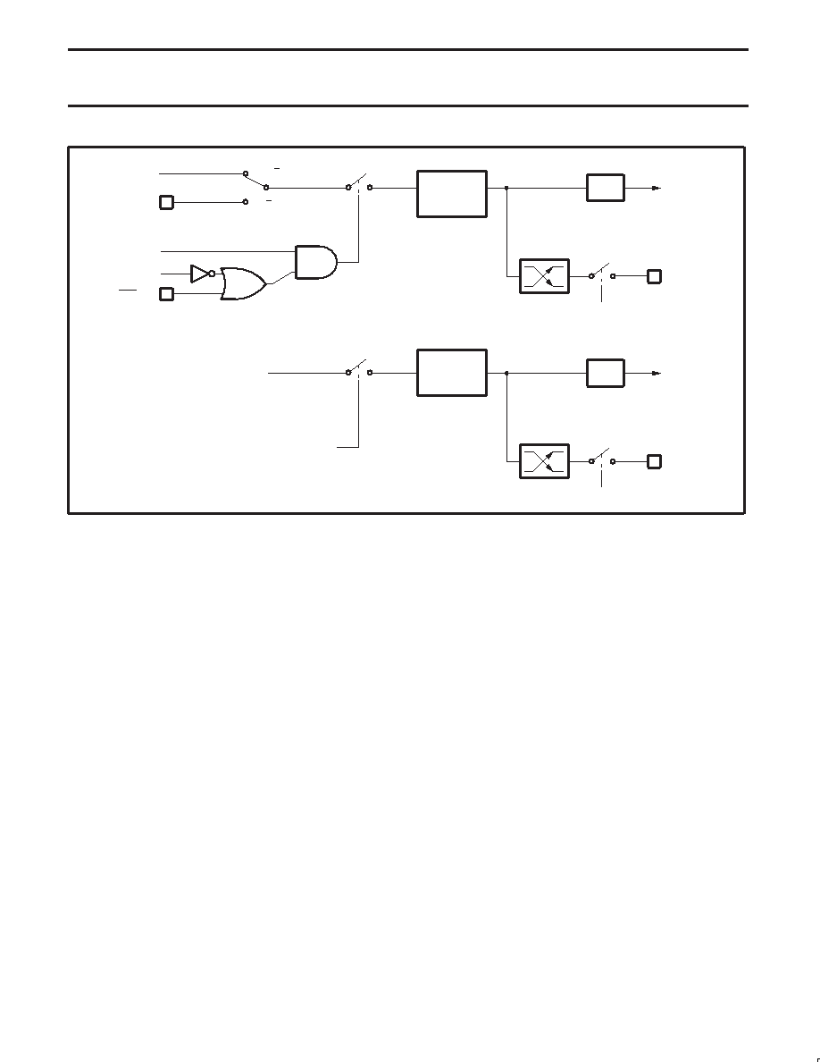
Figure 29. Timer/Counter 0 Mode 3 (Two 8-Bit Counters)
Timer Overflow Toggle Output
Timers 0 and 1 can be configured to automatically toggle a port
output whenever a timer overflow occurs. The same device pins that
are used for the T0 and T1 count inputs are also used for the timer
toggle outputs. This function is enabled by control bits T0OE and
T1OE in the P2M1 register, and apply to Timer 0 and Timer 1
respectively. The port outputs will be a logic 1 prior to the first timer
overflow when this mode is turned on.
UART
The P87LPC767 includes an enhanced 80C51 UART. The baud rate
source for the UART is timer 1 for modes 1 and 3, while the rate is
fixed in modes 0 and 2. Because CPU clocking is different on the
P87LPC767 than on the standard 80C51, baud rate calculation is
somewhat different. Enhancements over the standard 80C51 UART
include Framing Error detection and automatic address recognition.
The serial port is full duplex, meaning it can transmit and receive
simultaneously. It is also receive-buffered, meaning it can
commence reception of a second byte before a previously received
byte has been read from the SBUF register. However, if the first byte
still hasn’t been read by the time reception of the second byte is
complete, the first byte will be lost. The serial port receive and
transmit registers are both accessed through Special Function
Register SBUF. Writing to SBUF loads the transmit register, and
reading SBUF accesses a physically separate receive register.
The serial port can be operated in 4 modes:
Mode 0
Serial data enters and exits through RxD. TxD outputs the shift
clock. 8 bits are transmitted or received, LSB first. The baud rate is
fixed at 1/6 of the CPU clock frequency.
Mode 1
10 bits are transmitted (through TxD) or received (through RxD): a
start bit (logical 0), 8 data bits (LSB first), and a stop bit (logical 1).
When data is received, the stop bit is stored in RB8 in Special
Function Register SCON. The baud rate is variable and is
determined by the Timer 1 overflow rate.
Mode 2
11 bits are transmitted (through TxD) or received (through RxD):
start bit (logical 0), 8 data bits (LSB first), a programmable 9th data
bit, and a stop bit (logical 1). When data is transmitted, the 9th data
bit (TB8 in SCON) can be assigned the value of 0 or 1. Or, for
example, the parity bit (P, in the PSW) could be moved into TB8.
When data is received, the 9th data bit goes into RB8 in Special
Function Register SCON, while the stop bit is ignored. The baud
rate is programmable to either 1/16 or 1/32 of the CPU clock
frequency, as determined by the SMOD1 bit in PCON.
Mode 3
11 bits are transmitted (through TxD) or received (through RxD): a
start bit (logical 0), 8 data bits (LSB first), a programmable 9th data
bit, and a stop bit (logical 1). In fact, Mode 3 is the same as Mode 2
in all respects except baud rate. The baud rate in Mode 3 is variable
and is determined by the Timer 1 overflow rate.
In all four modes, transmission is initiated by any instruction that
uses SBUF as a destination register. Reception is initiated in Mode 0
by the condition RI = 0 and REN = 1. Reception is initiated in the
other modes by the incoming start bit if REN = 1.
相关PDF资料 |
PDF描述 |
|---|---|
| PIC24FJ128GA006-I/PT | IC PIC MCU FLASH 128K 64TQFP |
| PIC18F66K22-I/PT | IC MCU 8BIT 64KB FLASH 64TQFP |
| PIC18LF65K80-I/PT | MCU PIC ECAN 32KB FLASH 64TQFP |
| PIC18F65K80-I/PT | MCU PIC 32KB FLASH 64TQFP |
| PIC16C745-I/SP | IC MCU OTP 8KX14 USB A/D 28DIP |
相关代理商/技术参数 |
参数描述 |
|---|---|
| PIC18F66J55T-I/PT | 功能描述:8位微控制器 -MCU 96KB FLSH 3936Bs RAM USB 2.0 nanoWatt RoHS:否 制造商:Silicon Labs 核心:8051 处理器系列:C8051F39x 数据总线宽度:8 bit 最大时钟频率:50 MHz 程序存储器大小:16 KB 数据 RAM 大小:1 KB 片上 ADC:Yes 工作电源电压:1.8 V to 3.6 V 工作温度范围:- 40 C to + 105 C 封装 / 箱体:QFN-20 安装风格:SMD/SMT |
| PIC18F66J60-I/PT | 功能描述:8位微控制器 -MCU 64KB FL 12KB RAM 10BASE-T RoHS:否 制造商:Silicon Labs 核心:8051 处理器系列:C8051F39x 数据总线宽度:8 bit 最大时钟频率:50 MHz 程序存储器大小:16 KB 数据 RAM 大小:1 KB 片上 ADC:Yes 工作电源电压:1.8 V to 3.6 V 工作温度范围:- 40 C to + 105 C 封装 / 箱体:QFN-20 安装风格:SMD/SMT |
| PIC18F66J60T-I/PT | 功能描述:8位微控制器 -MCU 64KB FL 12KB RAM 10BASE-T RoHS:否 制造商:Silicon Labs 核心:8051 处理器系列:C8051F39x 数据总线宽度:8 bit 最大时钟频率:50 MHz 程序存储器大小:16 KB 数据 RAM 大小:1 KB 片上 ADC:Yes 工作电源电压:1.8 V to 3.6 V 工作温度范围:- 40 C to + 105 C 封装 / 箱体:QFN-20 安装风格:SMD/SMT |
| PIC18F66J65-I/PT | 功能描述:8位微控制器 -MCU 96KB FL 12KB RAM 10BASE-T RoHS:否 制造商:Silicon Labs 核心:8051 处理器系列:C8051F39x 数据总线宽度:8 bit 最大时钟频率:50 MHz 程序存储器大小:16 KB 数据 RAM 大小:1 KB 片上 ADC:Yes 工作电源电压:1.8 V to 3.6 V 工作温度范围:- 40 C to + 105 C 封装 / 箱体:QFN-20 安装风格:SMD/SMT |
| PIC18F66J65T-I/PT | 功能描述:8位微控制器 -MCU 96KB FL 12KB RAM 10BASE-T RoHS:否 制造商:Silicon Labs 核心:8051 处理器系列:C8051F39x 数据总线宽度:8 bit 最大时钟频率:50 MHz 程序存储器大小:16 KB 数据 RAM 大小:1 KB 片上 ADC:Yes 工作电源电压:1.8 V to 3.6 V 工作温度范围:- 40 C to + 105 C 封装 / 箱体:QFN-20 安装风格:SMD/SMT |
发布紧急采购,3分钟左右您将得到回复。