- 您现在的位置:买卖IC网 > PDF目录3812 > PIC18F8520-I/PT (Microchip Technology)IC MCU FLASH 16KX16 EEPROM80TQFP PDF资料下载
参数资料
| 型号: | PIC18F8520-I/PT |
| 厂商: | Microchip Technology |
| 文件页数: | 140/165页 |
| 文件大小: | 0K |
| 描述: | IC MCU FLASH 16KX16 EEPROM80TQFP |
| 产品培训模块: | Asynchronous Stimulus 8-bit PIC® Microcontroller Portfolio |
| 标准包装: | 119 |
| 系列: | PIC® 18F |
| 核心处理器: | PIC |
| 芯体尺寸: | 8-位 |
| 速度: | 40MHz |
| 连通性: | EBI/EMI,I²C,SPI,UART/USART |
| 外围设备: | 欠压检测/复位,LVD,POR,PWM,WDT |
| 输入/输出数: | 68 |
| 程序存储器容量: | 32KB(16K x 16) |
| 程序存储器类型: | 闪存 |
| EEPROM 大小: | 1K x 8 |
| RAM 容量: | 2K x 8 |
| 电压 - 电源 (Vcc/Vdd): | 4.2 V ~ 5.5 V |
| 数据转换器: | A/D 16x10b |
| 振荡器型: | 内部 |
| 工作温度: | -40°C ~ 85°C |
| 封装/外壳: | 80-TQFP |
| 包装: | 托盘 |
| 产品目录页面: | 643 (CN2011-ZH PDF) |
| 配用: | XLT80PT3-ND - SOCKET TRAN ICE 80MQFP/TQFP AC164320-ND - MODULE SKT MPLAB PM3 80TQFP AC174011-ND - MODULE SKT PROMATEII 80TQFP |
第1页第2页第3页第4页第5页第6页第7页第8页第9页第10页第11页第12页第13页第14页第15页第16页第17页第18页第19页第20页第21页第22页第23页第24页第25页第26页第27页第28页第29页第30页第31页第32页第33页第34页第35页第36页第37页第38页第39页第40页第41页第42页第43页第44页第45页第46页第47页第48页第49页第50页第51页第52页第53页第54页第55页第56页第57页第58页第59页第60页第61页第62页第63页第64页第65页第66页第67页第68页第69页第70页第71页第72页第73页第74页第75页第76页第77页第78页第79页第80页第81页第82页第83页第84页第85页第86页第87页第88页第89页第90页第91页第92页第93页第94页第95页第96页第97页第98页第99页第100页第101页第102页第103页第104页第105页第106页第107页第108页第109页第110页第111页第112页第113页第114页第115页第116页第117页第118页第119页第120页第121页第122页第123页第124页第125页第126页第127页第128页第129页第130页第131页第132页第133页第134页第135页第136页第137页第138页第139页当前第140页第141页第142页第143页第144页第145页第146页第147页第148页第149页第150页第151页第152页第153页第154页第155页第156页第157页第158页第159页第160页第161页第162页第163页第164页第165页
PIC18F6520/8520/6620/8620/6720/8720
DS39609B-page 74
2004 Microchip Technology Inc.
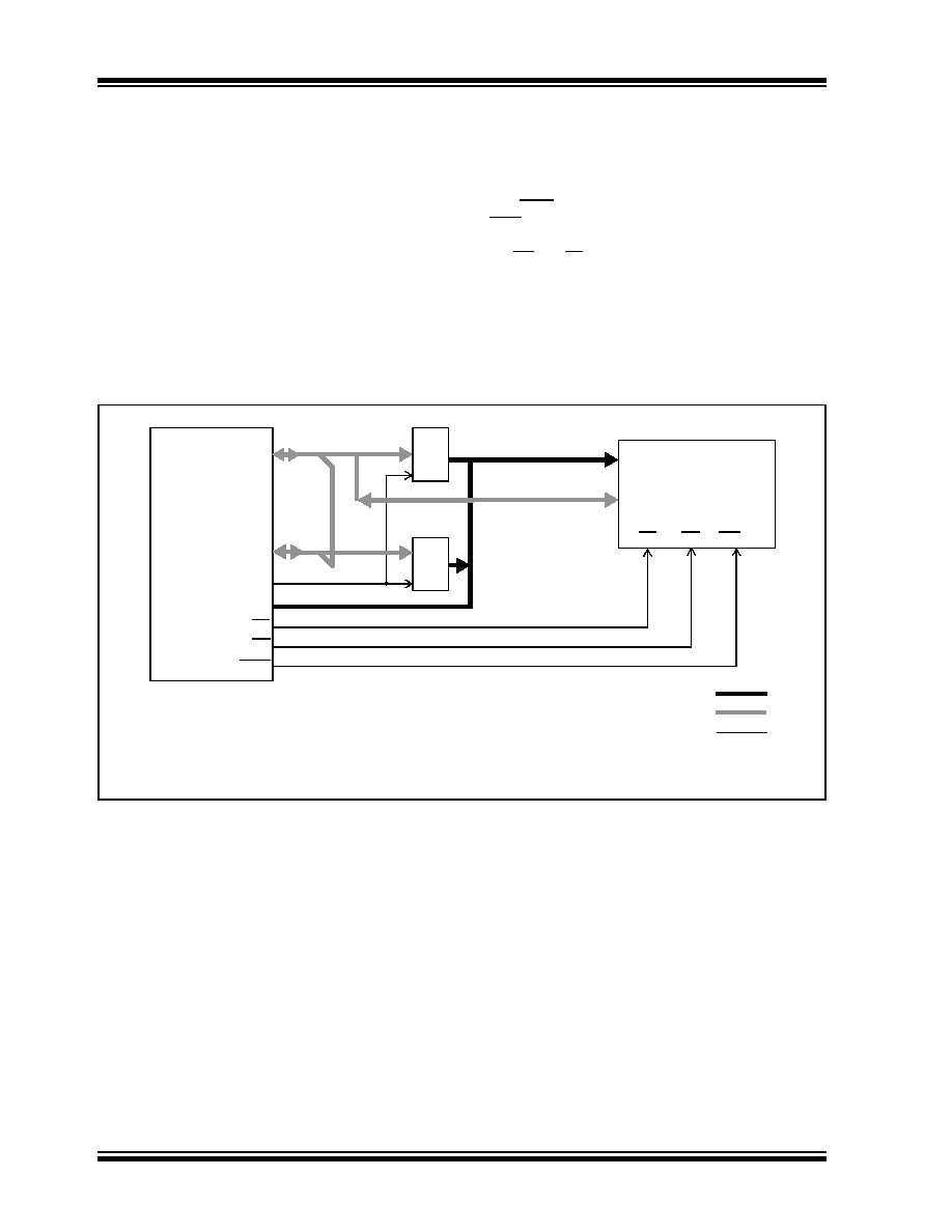
6.2.2
16-BIT WORD WRITE MODE
Figure 6-2 shows an example of 16-bit Word Write
mode for PIC18F8X20 devices. This mode is used for
word-wide memories, which includes some of the
EPROM and Flash type memories. This mode allows
opcode fetches and table reads from all forms of 16-bit
memory and table writes to any type of word-wide
external memories. This method makes a distinction
between TBLWT cycles to even or odd addresses.
During
a
TBLWT
cycle
to
an
even
address
(TBLPTR<0> = 0), the TABLAT data is transferred to a
holding latch and the external address data bus is
tri-stated for the data portion of the bus cycle. No write
signals are activated.
During
a
TBLWT
cycle
to
an
odd
address
(TBLPTR<0> = 1), the TABLAT data is presented on
the upper byte of the AD15:AD0 bus. The contents of
the holding latch are presented on the lower byte of the
AD15:AD0 bus.
The WRH signal is strobed for each write cycle; the
WRL pin is unused. The signal on the BA0 pin indicates
the LSb of TBLPTR, but it is left unconnected. Instead,
the UB and LB signals are active to select both bytes.
The obvious limitation to this method is that the table
write must be done in pairs on a specific word boundary
to correctly write a word location.
FIGURE 6-2:
16-BIT WORD WRITE MODE EXAMPLE
AD<7:0>
PIC18F8X20
AD<15:8>
ALE
373
A<20:1>
373
OE
WRH
A<19:16>
A<x:0>
D<15:0>
OE
WR(1)
CE
D<15:0>
JEDEC Word
EPROM Memory
Address Bus
Data Bus
Control Lines
Note 1:
This signal only applies to table writes. See Section 5.1 “Table Reads and Table Writes”.
CE
相关PDF资料 |
PDF描述 |
|---|---|
| PIC16C74A-04/P | IC MCU OTP 4KX14 A/D PWM 40DIP |
| 202173-7 | CONN GUIDE PIN CORNER 104CF POS |
| PIC32MX664F128L-I/BG | MCU PIC 128KB FLASH 121XBGA |
| PIC24FJ256DA210-I/PT | MCU PIC 16BIT FLASH 256K 100TQFP |
| PIC18LF6520-I/PT | IC MCU FLASH 16KX16 EEPROM64TQFP |
相关代理商/技术参数 |
参数描述 |
|---|---|
| PIC18F8520T-E/PT | 功能描述:8位微控制器 -MCU 40MHz 32KB Flash RoHS:否 制造商:Silicon Labs 核心:8051 处理器系列:C8051F39x 数据总线宽度:8 bit 最大时钟频率:50 MHz 程序存储器大小:16 KB 数据 RAM 大小:1 KB 片上 ADC:Yes 工作电源电压:1.8 V to 3.6 V 工作温度范围:- 40 C to + 105 C 封装 / 箱体:QFN-20 安装风格:SMD/SMT |
| PIC18F8520T-I/PT | 功能描述:8位微控制器 -MCU 32KB 2048 RAM 68I/O RoHS:否 制造商:Silicon Labs 核心:8051 处理器系列:C8051F39x 数据总线宽度:8 bit 最大时钟频率:50 MHz 程序存储器大小:16 KB 数据 RAM 大小:1 KB 片上 ADC:Yes 工作电源电压:1.8 V to 3.6 V 工作温度范围:- 40 C to + 105 C 封装 / 箱体:QFN-20 安装风格:SMD/SMT |
| PIC18F8520T-I/PTG | 功能描述:8位微控制器 -MCU 32KB 2048 RAM 68I/O Lead Free Package RoHS:否 制造商:Silicon Labs 核心:8051 处理器系列:C8051F39x 数据总线宽度:8 bit 最大时钟频率:50 MHz 程序存储器大小:16 KB 数据 RAM 大小:1 KB 片上 ADC:Yes 工作电源电压:1.8 V to 3.6 V 工作温度范围:- 40 C to + 105 C 封装 / 箱体:QFN-20 安装风格:SMD/SMT |
| PIC18F8525-E/PT | 功能描述:8位微控制器 -MCU 48KB 3840 RAM 68I/O RoHS:否 制造商:Silicon Labs 核心:8051 处理器系列:C8051F39x 数据总线宽度:8 bit 最大时钟频率:50 MHz 程序存储器大小:16 KB 数据 RAM 大小:1 KB 片上 ADC:Yes 工作电源电压:1.8 V to 3.6 V 工作温度范围:- 40 C to + 105 C 封装 / 箱体:QFN-20 安装风格:SMD/SMT |
| PIC18F8525-I/PT | 功能描述:8位微控制器 -MCU 48KB 3840 RAM 68I/O RoHS:否 制造商:Silicon Labs 核心:8051 处理器系列:C8051F39x 数据总线宽度:8 bit 最大时钟频率:50 MHz 程序存储器大小:16 KB 数据 RAM 大小:1 KB 片上 ADC:Yes 工作电源电压:1.8 V to 3.6 V 工作温度范围:- 40 C to + 105 C 封装 / 箱体:QFN-20 安装风格:SMD/SMT |
发布紧急采购,3分钟左右您将得到回复。