- 您现在的位置:买卖IC网 > PDF目录299771 > PIC18LF1220-I/P 8-BIT, FLASH, 40 MHz, MICROCONTROLLER, PDIP18 PDF资料下载
参数资料
| 型号: | PIC18LF1220-I/P |
| 元件分类: | 微控制器/微处理器 |
| 英文描述: | 8-BIT, FLASH, 40 MHz, MICROCONTROLLER, PDIP18 |
| 封装: | 0.300 INCH, PLASTIC, MS-001, DIP-18 |
| 文件页数: | 11/310页 |
| 文件大小: | 5377K |
| 代理商: | PIC18LF1220-I/P |
第1页第2页第3页第4页第5页第6页第7页第8页第9页第10页当前第11页第12页第13页第14页第15页第16页第17页第18页第19页第20页第21页第22页第23页第24页第25页第26页第27页第28页第29页第30页第31页第32页第33页第34页第35页第36页第37页第38页第39页第40页第41页第42页第43页第44页第45页第46页第47页第48页第49页第50页第51页第52页第53页第54页第55页第56页第57页第58页第59页第60页第61页第62页第63页第64页第65页第66页第67页第68页第69页第70页第71页第72页第73页第74页第75页第76页第77页第78页第79页第80页第81页第82页第83页第84页第85页第86页第87页第88页第89页第90页第91页第92页第93页第94页第95页第96页第97页第98页第99页第100页第101页第102页第103页第104页第105页第106页第107页第108页第109页第110页第111页第112页第113页第114页第115页第116页第117页第118页第119页第120页第121页第122页第123页第124页第125页第126页第127页第128页第129页第130页第131页第132页第133页第134页第135页第136页第137页第138页第139页第140页第141页第142页第143页第144页第145页第146页第147页第148页第149页第150页第151页第152页第153页第154页第155页第156页第157页第158页第159页第160页第161页第162页第163页第164页第165页第166页第167页第168页第169页第170页第171页第172页第173页第174页第175页第176页第177页第178页第179页第180页第181页第182页第183页第184页第185页第186页第187页第188页第189页第190页第191页第192页第193页第194页第195页第196页第197页第198页第199页第200页第201页第202页第203页第204页第205页第206页第207页第208页第209页第210页第211页第212页第213页第214页第215页第216页第217页第218页第219页第220页第221页第222页第223页第224页第225页第226页第227页第228页第229页第230页第231页第232页第233页第234页第235页第236页第237页第238页第239页第240页第241页第242页第243页第244页第245页第246页第247页第248页第249页第250页第251页第252页第253页第254页第255页第256页第257页第258页第259页第260页第261页第262页第263页第264页第265页第266页第267页第268页第269页第270页第271页第272页第273页第274页第275页第276页第277页第278页第279页第280页第281页第282页第283页第284页第285页第286页第287页第288页第289页第290页第291页第292页第293页第294页第295页第296页第297页第298页第299页第300页第301页第302页第303页第304页第305页第306页第307页第308页第309页第310页
PIC18F1220/1320
DS39605C-page 106
2004 Microchip Technology Inc.
12.3
Timer1 Oscillator Layout
Considerations
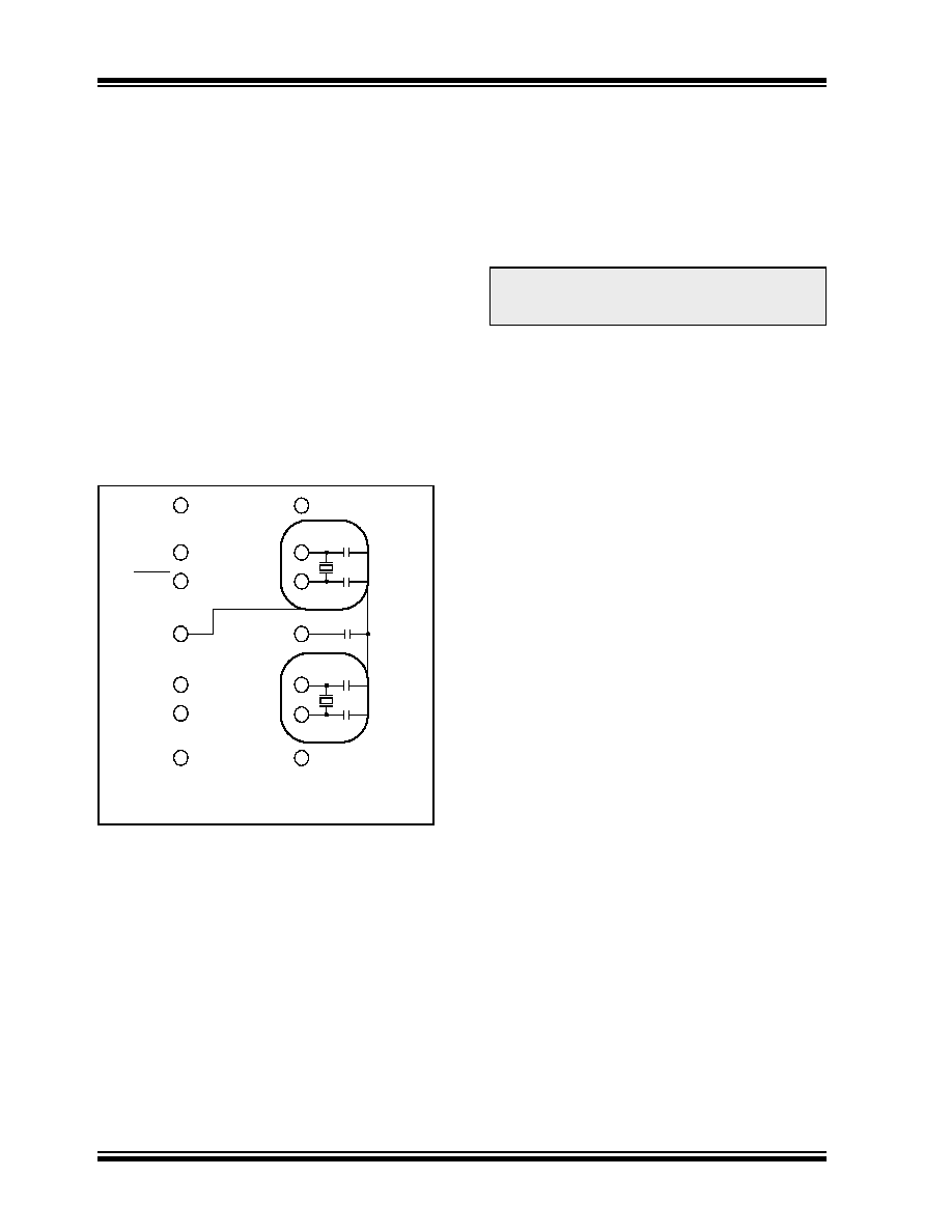
The Timer1 oscillator circuit draws very little power
during operation. Due to the low-power nature of the
oscillator, it may also be sensitive to rapidly changing
signals in close proximity.
The oscillator circuit, shown in Figure 12-3, should be
located as close as possible to the microcontroller.
There should be no circuits passing within the oscillator
circuit boundaries other than VSS or VDD.
If a high-speed circuit must be located near the oscilla-
tor (such as the CCP1 pin in output compare or PWM
mode, or the primary oscillator using the OSC2 pin), a
grounded guard ring around the oscillator circuit, as
shown in Figure 12-4, may be helpful when used on a
single sided PCB, or in addition to a ground plane.
FIGURE 12-4:
OSCILLATOR CIRCUIT
WITH GROUNDED
GUARD RING
12.4
Timer1 Interrupt
The TMR1 register pair (TMR1H:TMR1L) increments
from 0000h to FFFFh and rolls over to 0000h. The
Timer1 interrupt, if enabled, is generated on overflow,
which is
latched in interrupt
flag
bit, TMR1IF
(PIR1<0>). This interrupt can be enabled/disabled by
setting/clearing Timer1 Interrupt Enable bit, TMR1IE
(PIE1<0>).
12.5
Resetting Timer1 Using a CCP
Trigger Output
If the CCP module is configured in Compare mode
to generate
a
“special
event
trigger”
(CCP1M3:CCP1M0 = 1011), this signal will reset
Timer1 and start an A/D conversion, if the A/D mod-
ule is enabled (see Section 15.4.4 “Special Event
Trigger” for more information).
Timer1 must be configured for either Timer or Synchro-
nized Counter mode to take advantage of this feature.
If Timer1 is running in Asynchronous Counter mode,
this Reset operation may not work.
In the event that a write to Timer1 coincides with a
special event trigger from CCP1, the write will take
precedence.
In this mode of operation, the CCPR1H:CCPR1L regis-
ter pair effectively becomes the period register for
Timer1.
12.6
Timer1 16-Bit Read/Write Mode
Timer1 can be configured for 16-bit reads and writes
(see
When
the
RD16
control
bit
(T1CON<7>) is set, the address for TMR1H is mapped
to a buffer register for the high byte of Timer1. A read
from TMR1L will load the contents of the high byte of
Timer1 into the Timer1 high byte buffer. This provides
the user with the ability to accurately read all 16 bits of
Timer1 without having to determine whether a read of
the high byte, followed by a read of the low byte, is
valid, due to a rollover between reads.
A write to the high byte of Timer1 must also take place
through the TMR1H Buffer register. Timer1 high byte is
updated with the contents of TMR1H when a write
occurs to TMR1L. This allows a user to write all 16 bits
to both the high and low bytes of Timer1 at once.
The high byte of Timer1 is not directly readable or
writable in this mode. All reads and writes must take
place through the Timer1 High Byte Buffer register.
Writes to TMR1H do not clear the Timer1 prescaler.
The prescaler is only cleared on writes to TMR1L.
RA1
RA4
RB0
MCLR
VSS
RA2
RA3
Note: Not drawn to scale.
RA3
RB2
OSC1
RB5
OSC2
VDD
RB7
RB6
C2
X1
C3
C4
X2
C5
C1
Note:
The special event triggers from the CCP1
module will not set interrupt flag bit,
TMR1IF (PIR1<0>).
相关PDF资料 |
PDF描述 |
|---|---|
| PIC18LF2320-I/SO | 8-BIT, FLASH, 40 MHz, MICROCONTROLLER, PDSO28 |
| PICO400AK | THUMB/PUSHWHEEL SWITCH-1SWITCHES, SPDT, 0.02A, 20VDC, THROUGH HOLE-STRAIGHT |
| PIO52-101KB | 1 ELEMENT, 100 uH, GENERAL PURPOSE INDUCTOR, SMD |
| PIO53-270MT | 1 ELEMENT, 27 uH, GENERAL PURPOSE INDUCTOR, SMD |
| PIO53-470MT | 1 ELEMENT, 47 uH, GENERAL PURPOSE INDUCTOR, SMD |
相关代理商/技术参数 |
参数描述 |
|---|---|
| PIC18LF1220ISS | 制造商:Microchip Technology Inc 功能描述: |
| PIC18LF1220T-I/ML | 功能描述:8位微控制器 -MCU 4KB 256 RAM 16I/O RoHS:否 制造商:Silicon Labs 核心:8051 处理器系列:C8051F39x 数据总线宽度:8 bit 最大时钟频率:50 MHz 程序存储器大小:16 KB 数据 RAM 大小:1 KB 片上 ADC:Yes 工作电源电压:1.8 V to 3.6 V 工作温度范围:- 40 C to + 105 C 封装 / 箱体:QFN-20 安装风格:SMD/SMT |
| PIC18LF1220T-I/SO | 功能描述:8位微控制器 -MCU 4KB 256 RAM 16I/O RoHS:否 制造商:Silicon Labs 核心:8051 处理器系列:C8051F39x 数据总线宽度:8 bit 最大时钟频率:50 MHz 程序存储器大小:16 KB 数据 RAM 大小:1 KB 片上 ADC:Yes 工作电源电压:1.8 V to 3.6 V 工作温度范围:- 40 C to + 105 C 封装 / 箱体:QFN-20 安装风格:SMD/SMT |
| PIC18LF1220T-I/SS | 功能描述:8位微控制器 -MCU 4KB 256 RAM 16I/O RoHS:否 制造商:Silicon Labs 核心:8051 处理器系列:C8051F39x 数据总线宽度:8 bit 最大时钟频率:50 MHz 程序存储器大小:16 KB 数据 RAM 大小:1 KB 片上 ADC:Yes 工作电源电压:1.8 V to 3.6 V 工作温度范围:- 40 C to + 105 C 封装 / 箱体:QFN-20 安装风格:SMD/SMT |
| PIC18LF1230-I/ML | 功能描述:8位微控制器 -MCU 4KB 256byt-R 16I/O RoHS:否 制造商:Silicon Labs 核心:8051 处理器系列:C8051F39x 数据总线宽度:8 bit 最大时钟频率:50 MHz 程序存储器大小:16 KB 数据 RAM 大小:1 KB 片上 ADC:Yes 工作电源电压:1.8 V to 3.6 V 工作温度范围:- 40 C to + 105 C 封装 / 箱体:QFN-20 安装风格:SMD/SMT |
发布紧急采购,3分钟左右您将得到回复。