- 您现在的位置:买卖IC网 > PDF目录299771 > PIC18LF1220T-I/SS 8-BIT, FLASH, 40 MHz, RISC MICROCONTROLLER, PDSO20 PDF资料下载
参数资料
| 型号: | PIC18LF1220T-I/SS |
| 元件分类: | 微控制器/微处理器 |
| 英文描述: | 8-BIT, FLASH, 40 MHz, RISC MICROCONTROLLER, PDSO20 |
| 封装: | 0.209 INCH, PLASTIC, MO-150, SSOP-20 |
| 文件页数: | 303/310页 |
| 文件大小: | 5377K |
| 代理商: | PIC18LF1220T-I/SS |
第1页第2页第3页第4页第5页第6页第7页第8页第9页第10页第11页第12页第13页第14页第15页第16页第17页第18页第19页第20页第21页第22页第23页第24页第25页第26页第27页第28页第29页第30页第31页第32页第33页第34页第35页第36页第37页第38页第39页第40页第41页第42页第43页第44页第45页第46页第47页第48页第49页第50页第51页第52页第53页第54页第55页第56页第57页第58页第59页第60页第61页第62页第63页第64页第65页第66页第67页第68页第69页第70页第71页第72页第73页第74页第75页第76页第77页第78页第79页第80页第81页第82页第83页第84页第85页第86页第87页第88页第89页第90页第91页第92页第93页第94页第95页第96页第97页第98页第99页第100页第101页第102页第103页第104页第105页第106页第107页第108页第109页第110页第111页第112页第113页第114页第115页第116页第117页第118页第119页第120页第121页第122页第123页第124页第125页第126页第127页第128页第129页第130页第131页第132页第133页第134页第135页第136页第137页第138页第139页第140页第141页第142页第143页第144页第145页第146页第147页第148页第149页第150页第151页第152页第153页第154页第155页第156页第157页第158页第159页第160页第161页第162页第163页第164页第165页第166页第167页第168页第169页第170页第171页第172页第173页第174页第175页第176页第177页第178页第179页第180页第181页第182页第183页第184页第185页第186页第187页第188页第189页第190页第191页第192页第193页第194页第195页第196页第197页第198页第199页第200页第201页第202页第203页第204页第205页第206页第207页第208页第209页第210页第211页第212页第213页第214页第215页第216页第217页第218页第219页第220页第221页第222页第223页第224页第225页第226页第227页第228页第229页第230页第231页第232页第233页第234页第235页第236页第237页第238页第239页第240页第241页第242页第243页第244页第245页第246页第247页第248页第249页第250页第251页第252页第253页第254页第255页第256页第257页第258页第259页第260页第261页第262页第263页第264页第265页第266页第267页第268页第269页第270页第271页第272页第273页第274页第275页第276页第277页第278页第279页第280页第281页第282页第283页第284页第285页第286页第287页第288页第289页第290页第291页第292页第293页第294页第295页第296页第297页第298页第299页第300页第301页第302页当前第303页第304页第305页第306页第307页第308页第309页第310页
PIC18F1220/1320
DS39605C-page 90
2004 Microchip Technology Inc.
10.2
PORTB, TRISB and LATB
Registers
PORTB is an 8-bit wide, bidirectional port. The corre-
sponding data direction register is TRISB. Setting a
TRISB bit (= 1) will make the corresponding PORTB
pin an input (i.e., put the corresponding output driver in
a high-impedance mode). Clearing a TRISB bit (= 0)
will make the corresponding PORTB pin an output (i.e.,
put the contents of the output latch on the selected pin).
The Data Latch register (LATB) is also memory
mapped. Read-modify-write operations on the LATB
register read and write the latched output value for
PORTB.
EXAMPLE 10-2:
INITIALIZING PORTB
Pins RB0-RB2 are multiplexed with INT0-INT2; pins
RB0, RB1 and RB4 are multiplexed with A/D inputs;
pins RB1 and RB4 are multiplexed with EUSART; and
pins RB2, RB3, RB6 and RB7 are multiplexed with
ECCP.
Each of the PORTB pins has a weak internal pull-up. A
single control bit can turn on all the pull-ups. This is
performed by clearing bit, RBPU (INTCON2<7>). The
weak pull-up is automatically turned off when the port
pin is configured as an output. The pull-ups are
disabled on a Power-on Reset.
Four of the PORTB pins (RB7:RB4) have an interrupt-
on-change feature. Only pins configured as inputs can
cause this interrupt to occur (i.e., any RB7:RB4 pin
configured as an output is excluded from the interrupt-
on-change comparison). The input pins (of RB7:RB4)
are compared with the old value latched on the last
read of PORTB. The “mismatch” outputs of RB7:RB4
are OR’ed together to generate the RB Port Change
Interrupt with Flag bit, RBIF (INTCON<0>).
This interrupt can wake the device from Sleep. The
user, in the Interrupt Service Routine, can clear the
interrupt in the following manner:
a)
Any read or write of PORTB (except with the
MOVFF
instruction). This will end the mismatch
condition.
b)
Clear flag bit, RBIF.
A mismatch condition will continue to set flag bit, RBIF.
Reading PORTB will end the mismatch condition and
allow flag bit, RBIF, to be cleared.
The interrupt-on-change feature is recommended for
wake-up on key depression operation and operations
where PORTB is only used for the interrupt-on-change
feature. Polling of PORTB is not recommended while
using the interrupt-on-change feature.
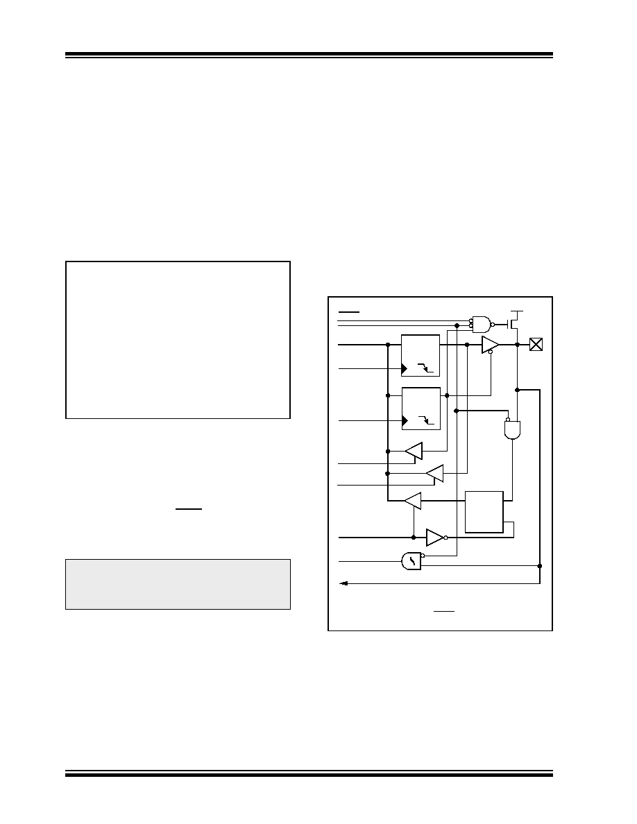
FIGURE 10-7:
BLOCK DIAGRAM OF
RB0/AN4/INT0 PIN
Note:
On a Power-on Reset, RB4:RB0 are
configured as analog inputs by default and
read as ‘0’; RB7:RB5 are configured as
digital inputs.
CLRF
PORTB
; Initialize PORTB by
; clearing output
; data latches
CLRF
LATB
; Alternate method
; to clear output
; data latches
MOVLW
0x70
; Set RB0, RB1, RB4 as
MOVWF
ADCON1
; digital I/O pins
MOVLW
0xCF
; Value used to
; initialize data
; direction
MOVWF
TRISB
; Set RB<3:0> as inputs
; RB<5:4> as outputs
; RB<7:6> as inputs
Data Latch
RBPU(2)
P
VDD
Data Bus
WR LATB
WR TRISB
RD TRISB
RD PORTB
Weak
Pull-up
INTx
I/O
pin(1)
Schmitt Trigger
Buffer
TRIS Latch
RD LATB
or PORTB
Note 1:
I/O pins have diode protection to VDD and VSS.
2:
To enable weak pull-ups, set the appropriate TRIS
bit(s) and clear the RBPU bit (INTCON2<7>).
To A/D Converter
Analog Input Mode
TTL
Input
Buffer
Q
D
CK
Q
D
CK
EN
QD
EN
相关PDF资料 |
PDF描述 |
|---|---|
| PIC18LF1220T-I/SO | 8-BIT, FLASH, 40 MHz, MICROCONTROLLER, PDSO18 |
| PIC18LF1220-I/P | 8-BIT, FLASH, 40 MHz, MICROCONTROLLER, PDIP18 |
| PIC18LF2320-I/SO | 8-BIT, FLASH, 40 MHz, MICROCONTROLLER, PDSO28 |
| PICO400AK | THUMB/PUSHWHEEL SWITCH-1SWITCHES, SPDT, 0.02A, 20VDC, THROUGH HOLE-STRAIGHT |
| PIO52-101KB | 1 ELEMENT, 100 uH, GENERAL PURPOSE INDUCTOR, SMD |
相关代理商/技术参数 |
参数描述 |
|---|---|
| PIC18LF1230-I/ML | 功能描述:8位微控制器 -MCU 4KB 256byt-R 16I/O RoHS:否 制造商:Silicon Labs 核心:8051 处理器系列:C8051F39x 数据总线宽度:8 bit 最大时钟频率:50 MHz 程序存储器大小:16 KB 数据 RAM 大小:1 KB 片上 ADC:Yes 工作电源电压:1.8 V to 3.6 V 工作温度范围:- 40 C to + 105 C 封装 / 箱体:QFN-20 安装风格:SMD/SMT |
| PIC18LF1230-I/P | 功能描述:8位微控制器 -MCU 4KB 256byt-RAM 16I/O RoHS:否 制造商:Silicon Labs 核心:8051 处理器系列:C8051F39x 数据总线宽度:8 bit 最大时钟频率:50 MHz 程序存储器大小:16 KB 数据 RAM 大小:1 KB 片上 ADC:Yes 工作电源电压:1.8 V to 3.6 V 工作温度范围:- 40 C to + 105 C 封装 / 箱体:QFN-20 安装风格:SMD/SMT |
| PIC18LF1230-I/SO | 功能描述:8位微控制器 -MCU 4KB 256byt-RAM 16I/O RoHS:否 制造商:Silicon Labs 核心:8051 处理器系列:C8051F39x 数据总线宽度:8 bit 最大时钟频率:50 MHz 程序存储器大小:16 KB 数据 RAM 大小:1 KB 片上 ADC:Yes 工作电源电压:1.8 V to 3.6 V 工作温度范围:- 40 C to + 105 C 封装 / 箱体:QFN-20 安装风格:SMD/SMT |
| PIC18LF1230-I/SS | 功能描述:8位微控制器 -MCU 4KBFlash 256byte-RAM 16 I/O 8-bit Family RoHS:否 制造商:Silicon Labs 核心:8051 处理器系列:C8051F39x 数据总线宽度:8 bit 最大时钟频率:50 MHz 程序存储器大小:16 KB 数据 RAM 大小:1 KB 片上 ADC:Yes 工作电源电压:1.8 V to 3.6 V 工作温度范围:- 40 C to + 105 C 封装 / 箱体:QFN-20 安装风格:SMD/SMT |
| PIC18LF1320-I/ML | 功能描述:8位微控制器 -MCU 8KB 256 RAM 16I/O RoHS:否 制造商:Silicon Labs 核心:8051 处理器系列:C8051F39x 数据总线宽度:8 bit 最大时钟频率:50 MHz 程序存储器大小:16 KB 数据 RAM 大小:1 KB 片上 ADC:Yes 工作电源电压:1.8 V to 3.6 V 工作温度范围:- 40 C to + 105 C 封装 / 箱体:QFN-20 安装风格:SMD/SMT |
发布紧急采购,3分钟左右您将得到回复。