- 您现在的位置:买卖IC网 > PDF目录268247 > PIC18LF24J10-E/SO 8-BIT, FLASH, 40 MHz, RISC MICROCONTROLLER, PDSO28 PDF资料下载
参数资料
| 型号: | PIC18LF24J10-E/SO |
| 元件分类: | 微控制器/微处理器 |
| 英文描述: | 8-BIT, FLASH, 40 MHz, RISC MICROCONTROLLER, PDSO28 |
| 封装: | 7.50 MM, PLASTIC, SOIC-28 |
| 文件页数: | 49/358页 |
| 文件大小: | 5679K |
| 代理商: | PIC18LF24J10-E/SO |
第1页第2页第3页第4页第5页第6页第7页第8页第9页第10页第11页第12页第13页第14页第15页第16页第17页第18页第19页第20页第21页第22页第23页第24页第25页第26页第27页第28页第29页第30页第31页第32页第33页第34页第35页第36页第37页第38页第39页第40页第41页第42页第43页第44页第45页第46页第47页第48页当前第49页第50页第51页第52页第53页第54页第55页第56页第57页第58页第59页第60页第61页第62页第63页第64页第65页第66页第67页第68页第69页第70页第71页第72页第73页第74页第75页第76页第77页第78页第79页第80页第81页第82页第83页第84页第85页第86页第87页第88页第89页第90页第91页第92页第93页第94页第95页第96页第97页第98页第99页第100页第101页第102页第103页第104页第105页第106页第107页第108页第109页第110页第111页第112页第113页第114页第115页第116页第117页第118页第119页第120页第121页第122页第123页第124页第125页第126页第127页第128页第129页第130页第131页第132页第133页第134页第135页第136页第137页第138页第139页第140页第141页第142页第143页第144页第145页第146页第147页第148页第149页第150页第151页第152页第153页第154页第155页第156页第157页第158页第159页第160页第161页第162页第163页第164页第165页第166页第167页第168页第169页第170页第171页第172页第173页第174页第175页第176页第177页第178页第179页第180页第181页第182页第183页第184页第185页第186页第187页第188页第189页第190页第191页第192页第193页第194页第195页第196页第197页第198页第199页第200页第201页第202页第203页第204页第205页第206页第207页第208页第209页第210页第211页第212页第213页第214页第215页第216页第217页第218页第219页第220页第221页第222页第223页第224页第225页第226页第227页第228页第229页第230页第231页第232页第233页第234页第235页第236页第237页第238页第239页第240页第241页第242页第243页第244页第245页第246页第247页第248页第249页第250页第251页第252页第253页第254页第255页第256页第257页第258页第259页第260页第261页第262页第263页第264页第265页第266页第267页第268页第269页第270页第271页第272页第273页第274页第275页第276页第277页第278页第279页第280页第281页第282页第283页第284页第285页第286页第287页第288页第289页第290页第291页第292页第293页第294页第295页第296页第297页第298页第299页第300页第301页第302页第303页第304页第305页第306页第307页第308页第309页第310页第311页第312页第313页第314页第315页第316页第317页第318页第319页第320页第321页第322页第323页第324页第325页第326页第327页第328页第329页第330页第331页第332页第333页第334页第335页第336页第337页第338页第339页第340页第341页第342页第343页第344页第345页第346页第347页第348页第349页第350页第351页第352页第353页第354页第355页第356页第357页第358页
PIC18F45J10 FAMILY
DS39682C-page 140
Preliminary
2007 Microchip Technology Inc.
14.4.6
PROGRAMMABLE DEAD-BAND
DELAY
In half-bridge applications, where all power switches
are modulated at the PWM frequency at all times, the
power switches normally require more time to turn off
than to turn on. If both the upper and lower power
switches are switched at the same time (one turned on
and the other turned off), both switches may be on for
a short period of time until one switch completely turns
off. During this brief interval, a very high current (shoot-
through current) may flow through both power
switches, shorting the bridge supply. To avoid this
potentially destructive shoot-through current from
flowing during switching, turning on either of the power
switches is normally delayed to allow the other switch
to completely turn off.
In the Half-Bridge Output mode, a digitally programmable
dead-band delay is available to avoid shoot-through
current from destroying the bridge power switches. The
delay occurs at the signal transition from the nonactive
state to the active state. See Figure 14-4 for an
illustration. Bits PDC6:PDC0 of the ECCP1DEL register
(Register 14-2) set the delay period in terms of microcon-
troller instruction cycles (TCY or 4 TOSC). These bits are
not available in 28-pin devices as the standard CCP
module does not support half-bridge operation.
14.4.7
ENHANCED PWM AUTO-SHUTDOWN
When the ECCP1 is programmed for any of the
Enhanced PWM modes, the active output pins may be
configured for auto-shutdown. Auto-shutdown immedi-
ately places the Enhanced PWM output pins into a
defined shutdown state when a shutdown event occurs.
A shutdown event can be caused by either of the
comparator modules, a low level on the Fault input pin
(FLT0) or any combination of these three sources. The
comparators may be used to monitor a voltage input
proportional to a current being monitored in the bridge
circuit. If the voltage exceeds a threshold, the
comparator switches state and triggers a shutdown.
Alternatively, a low digital signal on FLT0 can also trigger
a shutdown. The auto-shutdown feature can be disabled
by not selecting any auto-shutdown sources. The auto-
shutdown sources to be used are selected using the
ECCPAS2:ECCPAS0 bits (bits<6:4> of the ECCP1AS
register).
When a shutdown occurs, the output pins are
asynchronously placed in their shutdown states, spec-
ified by the PSSAC1:PSSAC0 and PSSBD1:PSSBD0
bits (ECCPAS3:ECCPAS0). Each pin pair (P1A/P1C
and P1B/P1D) may be set to drive high, drive low or be
tri-stated
(not
driving).
The
ECCPASE
bit
(ECCP1AS<7>) is also set to hold the Enhanced PWM
outputs in their shutdown states.
The ECCPASE bit is set by hardware when a shutdown
event occurs. If automatic restarts are not enabled, the
ECCPASE bit is cleared by firmware when the cause of
the shutdown clears. If automatic restarts are enabled,
the ECCPASE bit is automatically cleared when the
cause of the auto-shutdown has cleared.
If the ECCPASE bit is set when a PWM period begins,
the PWM outputs remain in their shutdown state for that
entire PWM period. When the ECCPASE bit is cleared,
the PWM outputs will return to normal operation at the
beginning of the next PWM period.
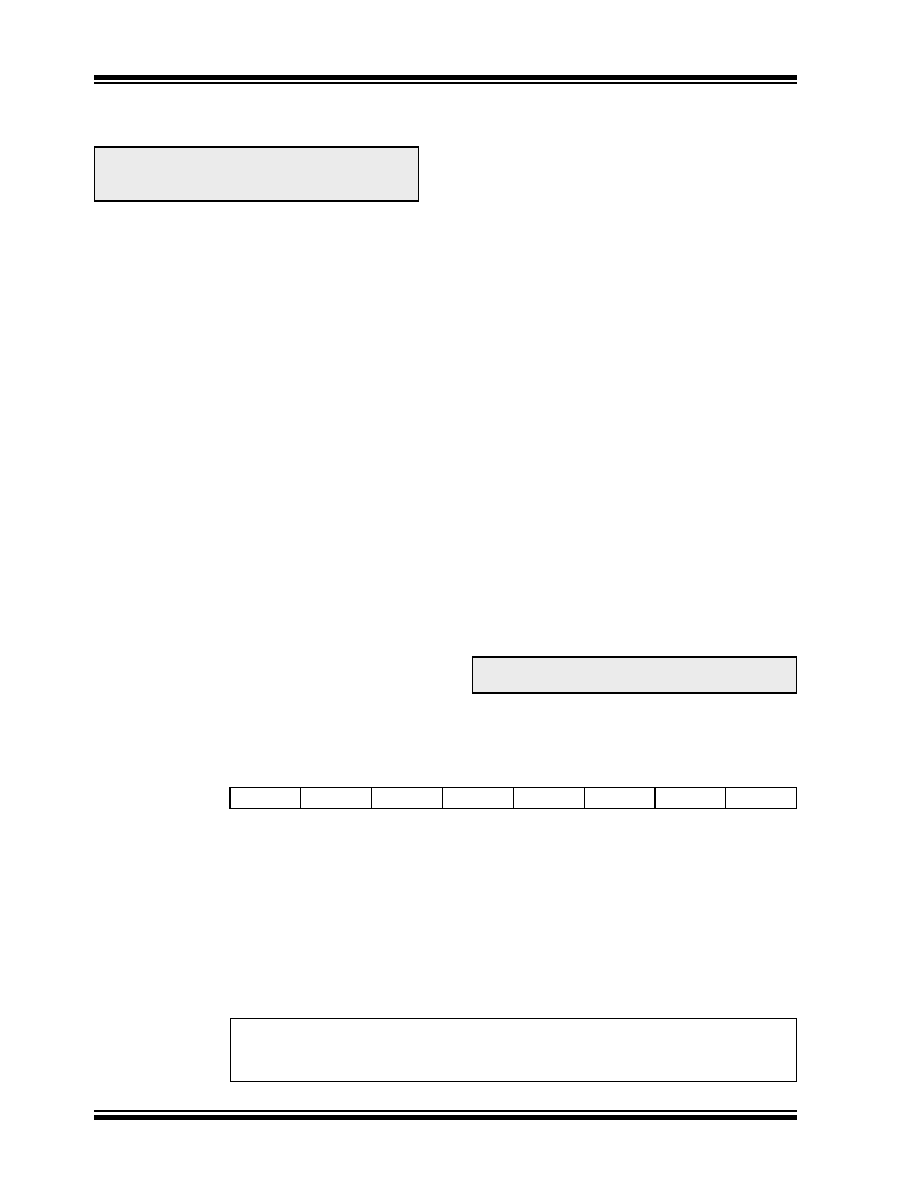
REGISTER 14-2:
ECCP1DEL: PWM DEAD-BAND DELAY REGISTER
Note:
Programmable dead-band delay is not
implemented
in
28-pin
devices
with
standard CCP modules.
Note:
Writing to the ECCPASE bit is disabled
while a shutdown condition is active.
R/W-0
PRSEN
PDC6(1)
PDC5(1)
PDC4(1)
PDC3(1)
PDC2(1)
PDC1(1)
PDC0(1)
bit 7
bit 0
bit 7
PRSEN: PWM Restart Enable bit
1
= Upon auto-shutdown, the ECCPASE bit clears automatically once the shutdown event
goes away; the PWM restarts automatically
0
= Upon auto-shutdown, ECCPASE must be cleared in software to restart the PWM
bit 6-0
PDC6:PDC0: PWM Delay Count bits(1)
Delay time, in number of FOSC/4 (4 * TOSC) cycles, between the scheduled and actual time for
a PWM signal to transition to active.
Note 1: Reserved on 28-pin devices; maintain these bits clear.
Legend:
R = Readable bit
W = Writable bit
U = Unimplemented bit, read as ‘0’
-n = Value at POR
‘1’ = Bit is set
‘0’ = Bit is cleared
x = Bit is unknown
相关PDF资料 |
PDF描述 |
|---|---|
| PIC16CR73-E/SP | 8-BIT, FLASH, 20 MHz, RISC MICROCONTROLLER, PDIP28 |
| PSD813F4-15JI | 128K X 8 FLASH, 27 I/O, PIA-GENERAL PURPOSE, PQCC52 |
| PSD813F4-15J | 128K X 8 FLASH, 27 I/O, PIA-GENERAL PURPOSE, PQCC52 |
| PSD813F4-70M | 128K X 8 FLASH, 27 I/O, PIA-GENERAL PURPOSE, PQFP52 |
| PIC16C57C-04E/SS | 8-BIT, OTPROM, 4 MHz, RISC MICROCONTROLLER, PDSO28 |
相关代理商/技术参数 |
参数描述 |
|---|---|
| PIC18LF24J10-I/ML | 功能描述:8位微控制器 -MCU 16 KB FL 1024 RAM RoHS:否 制造商:Silicon Labs 核心:8051 处理器系列:C8051F39x 数据总线宽度:8 bit 最大时钟频率:50 MHz 程序存储器大小:16 KB 数据 RAM 大小:1 KB 片上 ADC:Yes 工作电源电压:1.8 V to 3.6 V 工作温度范围:- 40 C to + 105 C 封装 / 箱体:QFN-20 安装风格:SMD/SMT |
| PIC18LF24J10-I/SO | 功能描述:8位微控制器 -MCU 16 KB FL 1024 RAM RoHS:否 制造商:Silicon Labs 核心:8051 处理器系列:C8051F39x 数据总线宽度:8 bit 最大时钟频率:50 MHz 程序存储器大小:16 KB 数据 RAM 大小:1 KB 片上 ADC:Yes 工作电源电压:1.8 V to 3.6 V 工作温度范围:- 40 C to + 105 C 封装 / 箱体:QFN-20 安装风格:SMD/SMT |
| PIC18LF24J10-I/SP | 功能描述:8位微控制器 -MCU 16 KB FL 1024 RAM RoHS:否 制造商:Silicon Labs 核心:8051 处理器系列:C8051F39x 数据总线宽度:8 bit 最大时钟频率:50 MHz 程序存储器大小:16 KB 数据 RAM 大小:1 KB 片上 ADC:Yes 工作电源电压:1.8 V to 3.6 V 工作温度范围:- 40 C to + 105 C 封装 / 箱体:QFN-20 安装风格:SMD/SMT |
| PIC18LF24J10-I/SS | 功能描述:8位微控制器 -MCU 16 KB FL 1024 RAM RoHS:否 制造商:Silicon Labs 核心:8051 处理器系列:C8051F39x 数据总线宽度:8 bit 最大时钟频率:50 MHz 程序存储器大小:16 KB 数据 RAM 大小:1 KB 片上 ADC:Yes 工作电源电压:1.8 V to 3.6 V 工作温度范围:- 40 C to + 105 C 封装 / 箱体:QFN-20 安装风格:SMD/SMT |
| PIC18LF24J10T-I/ML | 功能描述:8位微控制器 -MCU 16 KB FL 1024 RAM RoHS:否 制造商:Silicon Labs 核心:8051 处理器系列:C8051F39x 数据总线宽度:8 bit 最大时钟频率:50 MHz 程序存储器大小:16 KB 数据 RAM 大小:1 KB 片上 ADC:Yes 工作电源电压:1.8 V to 3.6 V 工作温度范围:- 40 C to + 105 C 封装 / 箱体:QFN-20 安装风格:SMD/SMT |
发布紧急采购,3分钟左右您将得到回复。