- 您现在的位置:买卖IC网 > PDF目录11746 > PIC18LF2510-I/SO (Microchip Technology)IC MCU FLASH 16KX16 28SOIC PDF资料下载
参数资料
| 型号: | PIC18LF2510-I/SO |
| 厂商: | Microchip Technology |
| 文件页数: | 45/234页 |
| 文件大小: | 0K |
| 描述: | IC MCU FLASH 16KX16 28SOIC |
| 产品培训模块: | Asynchronous Stimulus 8-bit PIC® Microcontroller Portfolio |
| 标准包装: | 27 |
| 系列: | PIC® 18F |
| 核心处理器: | PIC |
| 芯体尺寸: | 8-位 |
| 速度: | 40MHz |
| 连通性: | I²C,SPI,UART/USART |
| 外围设备: | 欠压检测/复位,HLVD,POR,PWM,WDT |
| 输入/输出数: | 25 |
| 程序存储器容量: | 32KB(16K x 16) |
| 程序存储器类型: | 闪存 |
| RAM 容量: | 1.5K x 8 |
| 电压 - 电源 (Vcc/Vdd): | 2 V ~ 5.5 V |
| 数据转换器: | A/D 10x10b |
| 振荡器型: | 内部 |
| 工作温度: | -40°C ~ 85°C |
| 封装/外壳: | 28-SOIC(0.295",7.50mm 宽) |
| 包装: | 管件 |
| 产品目录页面: | 643 (CN2011-ZH PDF) |
第1页第2页第3页第4页第5页第6页第7页第8页第9页第10页第11页第12页第13页第14页第15页第16页第17页第18页第19页第20页第21页第22页第23页第24页第25页第26页第27页第28页第29页第30页第31页第32页第33页第34页第35页第36页第37页第38页第39页第40页第41页第42页第43页第44页当前第45页第46页第47页第48页第49页第50页第51页第52页第53页第54页第55页第56页第57页第58页第59页第60页第61页第62页第63页第64页第65页第66页第67页第68页第69页第70页第71页第72页第73页第74页第75页第76页第77页第78页第79页第80页第81页第82页第83页第84页第85页第86页第87页第88页第89页第90页第91页第92页第93页第94页第95页第96页第97页第98页第99页第100页第101页第102页第103页第104页第105页第106页第107页第108页第109页第110页第111页第112页第113页第114页第115页第116页第117页第118页第119页第120页第121页第122页第123页第124页第125页第126页第127页第128页第129页第130页第131页第132页第133页第134页第135页第136页第137页第138页第139页第140页第141页第142页第143页第144页第145页第146页第147页第148页第149页第150页第151页第152页第153页第154页第155页第156页第157页第158页第159页第160页第161页第162页第163页第164页第165页第166页第167页第168页第169页第170页第171页第172页第173页第174页第175页第176页第177页第178页第179页第180页第181页第182页第183页第184页第185页第186页第187页第188页第189页第190页第191页第192页第193页第194页第195页第196页第197页第198页第199页第200页第201页第202页第203页第204页第205页第206页第207页第208页第209页第210页第211页第212页第213页第214页第215页第216页第217页第218页第219页第220页第221页第222页第223页第224页第225页第226页第227页第228页第229页第230页第231页第232页第233页第234页
2009 Microchip Technology Inc.
DS39636D-page 141
PIC18F2X1X/4X1X
15.4
Enhanced PWM Mode
The Enhanced PWM mode provides additional PWM
output options for a broader range of control applica-
tions. The module is a backward compatible version of
the standard CCP module and offers up to four outputs,
designated P1A through P1D. Users are also able to
select the polarity of the signal (either active-high or
active-low). The module’s output mode and polarity are
configured
by
setting
the
P1M1:P1M0
and
CCP1M3:CCP1M0 bits of the CCP1CON register.
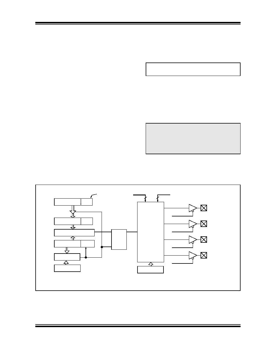
Figure 15-1 shows a simplified block diagram of PWM
operation. All control registers are double-buffered and
are loaded at the beginning of a new PWM cycle (the
period boundary when Timer2 resets) in order to
prevent glitches on any of the outputs. The exception is
the PWM Delay register, PWM1CON, which is loaded
at either the duty cycle boundary or the period bound-
ary (whichever comes first). Because of the buffering,
the module waits until the assigned timer resets instead
of starting immediately. This means that Enhanced
PWM waveforms do not exactly match the standard
PWM waveforms, but are instead offset by one full
instruction cycle (4 TOSC).
As before, the user must manually configure the
appropriate TRIS bits for output.
15.4.1
PWM PERIOD
The PWM period is specified by writing to the PR2
register. The PWM period can be calculated using the
following equation.
EQUATION 15-1:
PWM frequency is defined as 1/[PWM period]. When
TMR2 is equal to PR2, the following three events occur
on the next increment cycle:
TMR2 is cleared
The CCP1 pin is set (if PWM duty cycle = 0%, the
CCP1 pin will not be set)
The PWM duty cycle is copied from CCPR1L into
CCPR1H
FIGURE 15-1:
SIMPLIFIED BLOCK DIAGRAM OF THE ENHANCED PWM MODULE
Note:
The Timer2 postscaler (see Section 12.0
“Timer2 Module”) is not used in the
determination of the PWM frequency. The
postscaler could be used to have a servo
update rate at a different frequency than
the PWM output.
PWM Period = [(PR2) + 1] 4 TOSC
(TMR2 Prescale Value)
CCPR1L
CCPR1H (Slave)
Comparator
TMR2
Comparator
PR2
(Note 1)
RQ
S
Duty Cycle Registers
CCP1CON<5:4>
Clear Timer,
set CCP1 pin and
latch D.C.
Note: The 8-bit TMR2 register is concatenated with the 2-bit internal Q clock, or 2 bits of the prescaler, to create the 10-bit time
base.
TRISx<x>
CCP1/P1A
TRISx<x>
P1B
TRISx<x>
P1D
Output
Controller
P1M1<1:0>
2
CCP1M<3:0>
4
PWM1CON
CCP1/P1A
P1B
P1C
P1D
P1C
相关PDF资料 |
PDF描述 |
|---|---|
| PIC24HJ64GP202-I/MM | IC PIC MCU FLASH 64K 28-QFN |
| VE-BTV-IX-F2 | CONVERTER MOD DC/DC 5.8V 75W |
| VE-BTV-IX-F1 | CONVERTER MOD DC/DC 5.8V 75W |
| DSPIC30F1010-20E/MM | IC DSPIC MCU/DSP 6K 28QFN |
| VE-BTV-IW-F4 | CONVERTER MOD DC/DC 5.8V 100W |
相关代理商/技术参数 |
参数描述 |
|---|---|
| PIC18LF2510T-I/ML | 功能描述:8位微控制器 -MCU 32KB 1536 RAM 25I/O RoHS:否 制造商:Silicon Labs 核心:8051 处理器系列:C8051F39x 数据总线宽度:8 bit 最大时钟频率:50 MHz 程序存储器大小:16 KB 数据 RAM 大小:1 KB 片上 ADC:Yes 工作电源电压:1.8 V to 3.6 V 工作温度范围:- 40 C to + 105 C 封装 / 箱体:QFN-20 安装风格:SMD/SMT |
| PIC18LF2510T-I/SO | 功能描述:8位微控制器 -MCU 32KB 1536 RAM 25I/O RoHS:否 制造商:Silicon Labs 核心:8051 处理器系列:C8051F39x 数据总线宽度:8 bit 最大时钟频率:50 MHz 程序存储器大小:16 KB 数据 RAM 大小:1 KB 片上 ADC:Yes 工作电源电压:1.8 V to 3.6 V 工作温度范围:- 40 C to + 105 C 封装 / 箱体:QFN-20 安装风格:SMD/SMT |
| PIC18LF2515-I/SO | 功能描述:8位微控制器 -MCU 48KB 1536 RAM 25I/O RoHS:否 制造商:Silicon Labs 核心:8051 处理器系列:C8051F39x 数据总线宽度:8 bit 最大时钟频率:50 MHz 程序存储器大小:16 KB 数据 RAM 大小:1 KB 片上 ADC:Yes 工作电源电压:1.8 V to 3.6 V 工作温度范围:- 40 C to + 105 C 封装 / 箱体:QFN-20 安装风格:SMD/SMT |
| PIC18LF2515-I/SP | 功能描述:8位微控制器 -MCU 48KB 1536 RAM 25I/O RoHS:否 制造商:Silicon Labs 核心:8051 处理器系列:C8051F39x 数据总线宽度:8 bit 最大时钟频率:50 MHz 程序存储器大小:16 KB 数据 RAM 大小:1 KB 片上 ADC:Yes 工作电源电压:1.8 V to 3.6 V 工作温度范围:- 40 C to + 105 C 封装 / 箱体:QFN-20 安装风格:SMD/SMT |
| PIC18LF2515T-I/SO | 功能描述:8位微控制器 -MCU 48KB 1536 RAM 25I/O RoHS:否 制造商:Silicon Labs 核心:8051 处理器系列:C8051F39x 数据总线宽度:8 bit 最大时钟频率:50 MHz 程序存储器大小:16 KB 数据 RAM 大小:1 KB 片上 ADC:Yes 工作电源电压:1.8 V to 3.6 V 工作温度范围:- 40 C to + 105 C 封装 / 箱体:QFN-20 安装风格:SMD/SMT |
发布紧急采购,3分钟左右您将得到回复。