- 您现在的位置:买卖IC网 > PDF目录11421 > PIC18LF2510T-I/SO (Microchip Technology)IC MCU FLASH 16KX16 28SOIC PDF资料下载
参数资料
| 型号: | PIC18LF2510T-I/SO |
| 厂商: | Microchip Technology |
| 文件页数: | 44/234页 |
| 文件大小: | 0K |
| 描述: | IC MCU FLASH 16KX16 28SOIC |
| 产品培训模块: | Asynchronous Stimulus |
| 标准包装: | 1,600 |
| 系列: | PIC® 18F |
| 核心处理器: | PIC |
| 芯体尺寸: | 8-位 |
| 速度: | 40MHz |
| 连通性: | I²C,SPI,UART/USART |
| 外围设备: | 欠压检测/复位,HLVD,POR,PWM,WDT |
| 输入/输出数: | 25 |
| 程序存储器容量: | 32KB(16K x 16) |
| 程序存储器类型: | 闪存 |
| RAM 容量: | 1.5K x 8 |
| 电压 - 电源 (Vcc/Vdd): | 2 V ~ 5.5 V |
| 数据转换器: | A/D 10x10b |
| 振荡器型: | 内部 |
| 工作温度: | -40°C ~ 85°C |
| 封装/外壳: | 28-SOIC(0.295",7.50mm 宽) |
| 包装: | 带卷 (TR) |
第1页第2页第3页第4页第5页第6页第7页第8页第9页第10页第11页第12页第13页第14页第15页第16页第17页第18页第19页第20页第21页第22页第23页第24页第25页第26页第27页第28页第29页第30页第31页第32页第33页第34页第35页第36页第37页第38页第39页第40页第41页第42页第43页当前第44页第45页第46页第47页第48页第49页第50页第51页第52页第53页第54页第55页第56页第57页第58页第59页第60页第61页第62页第63页第64页第65页第66页第67页第68页第69页第70页第71页第72页第73页第74页第75页第76页第77页第78页第79页第80页第81页第82页第83页第84页第85页第86页第87页第88页第89页第90页第91页第92页第93页第94页第95页第96页第97页第98页第99页第100页第101页第102页第103页第104页第105页第106页第107页第108页第109页第110页第111页第112页第113页第114页第115页第116页第117页第118页第119页第120页第121页第122页第123页第124页第125页第126页第127页第128页第129页第130页第131页第132页第133页第134页第135页第136页第137页第138页第139页第140页第141页第142页第143页第144页第145页第146页第147页第148页第149页第150页第151页第152页第153页第154页第155页第156页第157页第158页第159页第160页第161页第162页第163页第164页第165页第166页第167页第168页第169页第170页第171页第172页第173页第174页第175页第176页第177页第178页第179页第180页第181页第182页第183页第184页第185页第186页第187页第188页第189页第190页第191页第192页第193页第194页第195页第196页第197页第198页第199页第200页第201页第202页第203页第204页第205页第206页第207页第208页第209页第210页第211页第212页第213页第214页第215页第216页第217页第218页第219页第220页第221页第222页第223页第224页第225页第226页第227页第228页第229页第230页第231页第232页第233页第234页
PIC18F2X1X/4X1X
DS39636D-page 140
2009 Microchip Technology Inc.
In addition to the expanded range of modes available
through the CCP1CON and ECCP1AS registers, the
ECCP module has an additional register associated
with Enhanced PWM operation and auto-shutdown
features. This register is:
PWM1CON (PWM Configuration register)
15.1
ECCP Outputs and Configuration
The Enhanced CCP module may have up to four PWM
outputs, depending on the selected operating mode.
These outputs, designated P1A through P1D, are
multiplexed with I/O pins on PORTC and PORTD. The
outputs that are active depend on the CCP operating
mode selected. The pin assignments are summarized
in Table 15-1.
To configure the I/O pins as PWM outputs, the proper
PWM mode must be selected by setting the
P1M1:P1M0
and
CCP1M3:CCP1M0
bits.
The
appropriate TRISC and TRISD direction bits for the port
pins must also be set as outputs.
15.1.1
ECCP MODULES AND TIMER
RESOURCES
Like the standard CCP modules, the ECCP module can
utilize Timers 1, 2 or 3, depending on the mode
selected. Timer1 and Timer3 are available for modules
in Capture or Compare modes, while Timer2 is
available for modules in PWM mode. Interactions
between the standard and Enhanced CCP modules are
identical to those described for standard CCP modules.
Additional details on timer resources are provided in
15.2
Capture and Compare Modes
Except for the operation of the special event trigger
discussed below, the Capture and Compare modes of
the ECCP module are identical in operation to that of
CCP2. These are discussed in detail in Section 14.2
Mode”. No changes are required when moving
between 28-pin and 40/44-pin devices.
15.2.1
SPECIAL EVENT TRIGGER
The special event trigger output of ECCP1 resets the
TMR1 or TMR3 register pair, depending on which timer
resource is currently selected. This allows the CCPR1
register to effectively be a 16-bit programmable period
register for Timer1 or Timer3.
15.3
Standard PWM Mode
When configured in Single Output mode, the ECCP
module functions identically to the standard CCP
module in PWM mode, as described in Section 14.4
“PWM Mode”. This is also sometimes referred to as
“Compatible CCP” mode, as in Table 15-1.
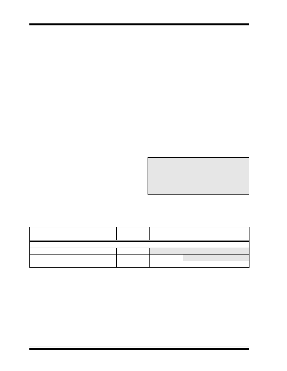
TABLE 15-1:
PIN ASSIGNMENTS FOR VARIOUS ECCP1 MODES
Note:
When setting up single output PWM
operations, users are free to use either of
the processes described in Section 14.4.4
or
tion”. The latter is more generic and will
work for either single or multi-output PWM.
ECCP Mode
CCP1CON
Configuration
RC2
RD5
RD6
RD7
All 40/44-pin devices:
Compatible CCP
00xx 11xx
CCP1
RD5/PSP5
RD6/PSP6
RD7/PSP7
Dual PWM
10xx 11xx
P1A
P1B
RD6/PSP6
RD7/PSP7
Quad PWM
x1xx 11xx
P1A
P1B
P1C
P1D
Legend: x = Don’t care. Shaded cells indicate pin assignments not used by ECCP1 in a given mode.
相关PDF资料 |
PDF描述 |
|---|---|
| PI2PCIE2422ZHE | IC MUX/DEMUX 2X1 42TQFN |
| PIC18F4420T-I/ML | IC MCU FLASH 8KX16 44QFN |
| PIC16F88-E/SO | IC MCU FLASH 4KX14 EEPROM 18SOIC |
| PIC16LF73T-I/SS | IC MCU FLASH 4KX14 A/D 28SSOP |
| PI5V330QE | IC VIDEO MUX/DEMUX 2X1 16QSOP |
相关代理商/技术参数 |
参数描述 |
|---|---|
| PIC18LF2515-I/SO | 功能描述:8位微控制器 -MCU 48KB 1536 RAM 25I/O RoHS:否 制造商:Silicon Labs 核心:8051 处理器系列:C8051F39x 数据总线宽度:8 bit 最大时钟频率:50 MHz 程序存储器大小:16 KB 数据 RAM 大小:1 KB 片上 ADC:Yes 工作电源电压:1.8 V to 3.6 V 工作温度范围:- 40 C to + 105 C 封装 / 箱体:QFN-20 安装风格:SMD/SMT |
| PIC18LF2515-I/SP | 功能描述:8位微控制器 -MCU 48KB 1536 RAM 25I/O RoHS:否 制造商:Silicon Labs 核心:8051 处理器系列:C8051F39x 数据总线宽度:8 bit 最大时钟频率:50 MHz 程序存储器大小:16 KB 数据 RAM 大小:1 KB 片上 ADC:Yes 工作电源电压:1.8 V to 3.6 V 工作温度范围:- 40 C to + 105 C 封装 / 箱体:QFN-20 安装风格:SMD/SMT |
| PIC18LF2515T-I/SO | 功能描述:8位微控制器 -MCU 48KB 1536 RAM 25I/O RoHS:否 制造商:Silicon Labs 核心:8051 处理器系列:C8051F39x 数据总线宽度:8 bit 最大时钟频率:50 MHz 程序存储器大小:16 KB 数据 RAM 大小:1 KB 片上 ADC:Yes 工作电源电压:1.8 V to 3.6 V 工作温度范围:- 40 C to + 105 C 封装 / 箱体:QFN-20 安装风格:SMD/SMT |
| PIC18LF2520-I/ML | 功能描述:8位微控制器 -MCU 32kBF 1536RM 25 I/O RoHS:否 制造商:Silicon Labs 核心:8051 处理器系列:C8051F39x 数据总线宽度:8 bit 最大时钟频率:50 MHz 程序存储器大小:16 KB 数据 RAM 大小:1 KB 片上 ADC:Yes 工作电源电压:1.8 V to 3.6 V 工作温度范围:- 40 C to + 105 C 封装 / 箱体:QFN-20 安装风格:SMD/SMT |
| PIC18LF2520-I/SO | 功能描述:8位微控制器 -MCU 32KB 1536 RAM 25I/O RoHS:否 制造商:Silicon Labs 核心:8051 处理器系列:C8051F39x 数据总线宽度:8 bit 最大时钟频率:50 MHz 程序存储器大小:16 KB 数据 RAM 大小:1 KB 片上 ADC:Yes 工作电源电压:1.8 V to 3.6 V 工作温度范围:- 40 C to + 105 C 封装 / 箱体:QFN-20 安装风格:SMD/SMT |
发布紧急采购,3分钟左右您将得到回复。