- 您现在的位置:买卖IC网 > PDF目录11749 > PIC18LF4221-I/ML (Microchip Technology)IC PIC MCU FLASH 2KX16 44QFN PDF资料下载
参数资料
| 型号: | PIC18LF4221-I/ML |
| 厂商: | Microchip Technology |
| 文件页数: | 48/110页 |
| 文件大小: | 0K |
| 描述: | IC PIC MCU FLASH 2KX16 44QFN |
| 产品培训模块: | Asynchronous Stimulus 8-bit PIC® Microcontroller Portfolio |
| 标准包装: | 45 |
| 系列: | PIC® 18F |
| 核心处理器: | PIC |
| 芯体尺寸: | 8-位 |
| 速度: | 40MHz |
| 连通性: | I²C,SPI,UART/USART |
| 外围设备: | 欠压检测/复位,HLVD,POR,PWM,WDT |
| 输入/输出数: | 36 |
| 程序存储器容量: | 4KB(2K x 16) |
| 程序存储器类型: | 闪存 |
| EEPROM 大小: | 256 x 8 |
| RAM 容量: | 512 x 8 |
| 电压 - 电源 (Vcc/Vdd): | 2 V ~ 5.5 V |
| 数据转换器: | A/D 13x10b |
| 振荡器型: | 内部 |
| 工作温度: | -40°C ~ 85°C |
| 封装/外壳: | 44-VQFN 裸露焊盘 |
| 包装: | 管件 |
| 产品目录页面: | 642 (CN2011-ZH PDF) |
第1页第2页第3页第4页第5页第6页第7页第8页第9页第10页第11页第12页第13页第14页第15页第16页第17页第18页第19页第20页第21页第22页第23页第24页第25页第26页第27页第28页第29页第30页第31页第32页第33页第34页第35页第36页第37页第38页第39页第40页第41页第42页第43页第44页第45页第46页第47页当前第48页第49页第50页第51页第52页第53页第54页第55页第56页第57页第58页第59页第60页第61页第62页第63页第64页第65页第66页第67页第68页第69页第70页第71页第72页第73页第74页第75页第76页第77页第78页第79页第80页第81页第82页第83页第84页第85页第86页第87页第88页第89页第90页第91页第92页第93页第94页第95页第96页第97页第98页第99页第100页第101页第102页第103页第104页第105页第106页第107页第108页第109页第110页
PIC18F2221/2321/4221/4321 FAMILY
DS39689F-page 42
2009 Microchip Technology Inc.
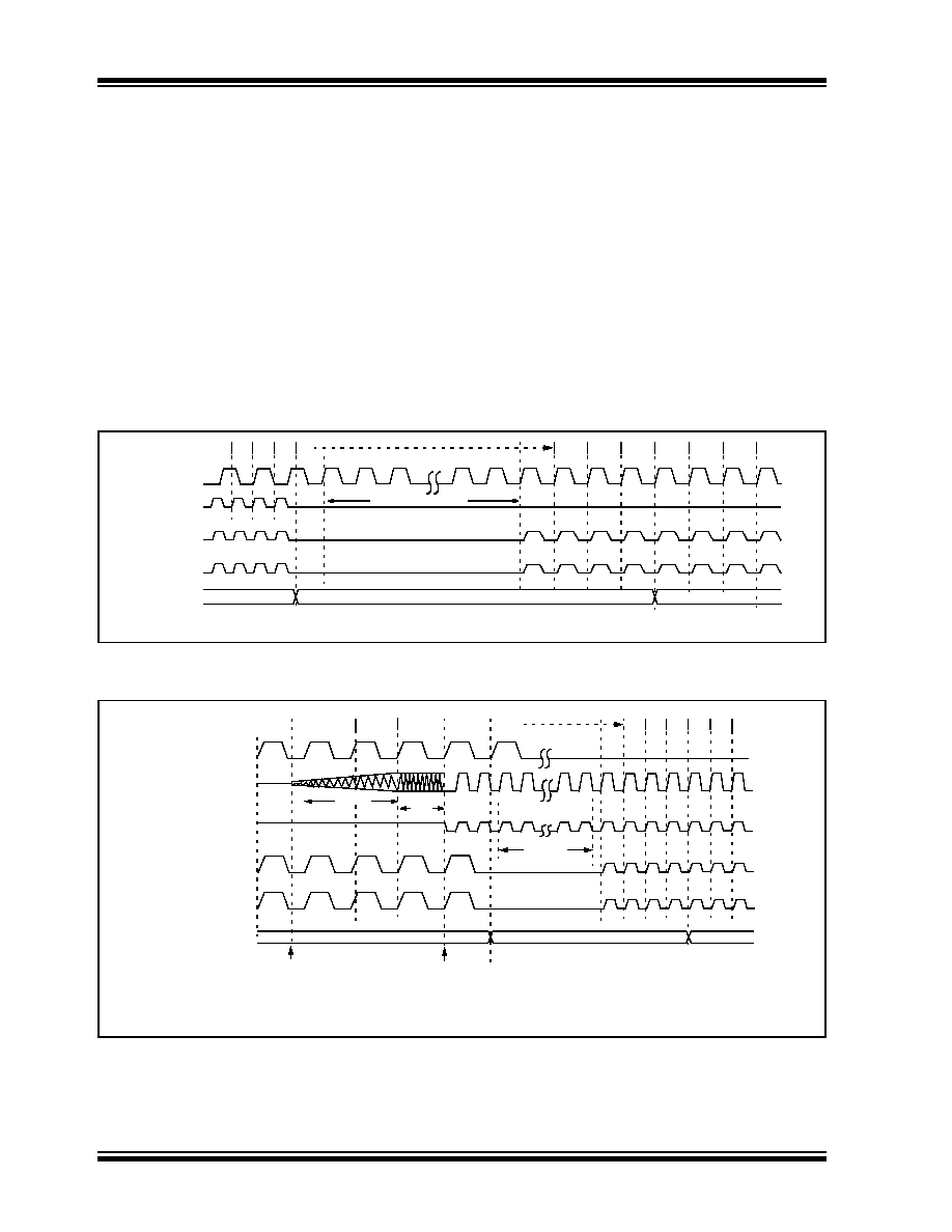
If the IRCF bits and the INTSRC bit are all clear, the
INTOSC output is not enabled and the IOFS bit will
remain clear; there will be no indication of the current
clock source. The INTRC source is providing the
device clocks.
If the IRCF bits are changed from all clear (thus,
enabling the INTOSC output) or if INTSRC is set, the
IOFS bit becomes set after the INTOSC output
becomes stable. Clocks to the device continue while
the INTOSC source stabilizes after an interval of
If the IRCF bits were previously at a non-zero value, or
if INTSRC was set before setting SCS1 and the
INTOSC source was already stable, the IOFS bit will
remain set.
On transitions from RC_RUN mode to PRI_RUN mode,
the device continues to be clocked from the INTOSC
multiplexer while the primary clock is started. When the
primary clock becomes ready, a clock switch to the
primary clock occurs (see Figure 4-4). When the clock
switch is complete, the IOFS bit is cleared, the OSTS
bit is set and the primary clock is providing the device
clock. The IDLEN and SCS bits are not affected by the
switch. The INTRC source will continue to run if either
the WDT or the Fail-Safe Clock Monitor is enabled.
FIGURE 4-3:
TRANSITION TIMING TO RC_RUN MODE
FIGURE 4-4:
TRANSITION TIMING FROM RC_RUN MODE TO PRI_RUN MODE
Q4
Q3
Q2
OSC1
Peripheral
Program
Q1
INTRC
Q1
Counter
Clock
CPU
Clock
PC + 2
PC
123
n-1
n
Clock Transition(1)
Q4
Q3
Q2
Q1
Q3
Q2
PC + 4
Note 1: Clock transition typically occurs within 2-4 TOSC.
Q1
Q3 Q4
OSC1
Peripheral
Program
PC
INTOSC
PLL Clock
Q1
PC + 4
Q2
Output
Q3
Q4
Q1
CPU Clock
PC + 2
Clock
Counter
Q2
Q3
Note 1: TOST = 1024 TOSC; TPLL = 2 ms (approx). These intervals are not shown to scale.
2: Clock transition typically occurs within 2-4 TOSC.
SCS<1:0> bits Changed
TPLL(1)
12
n-1 n
Clock
OSTS bit Set
Transition(2)
Multiplexer
TOST(1)
相关PDF资料 |
PDF描述 |
|---|---|
| VE-B4D-IX-F3 | CONVERTER MOD DC/DC 85V 75W |
| UPL2000-D19 | BNC PLUG CRIMP STR BELDEN 1855A |
| UPL2000-D1 | BNC PLUG CRIMP STR 7538 CABLE |
| DSPIC33FJ32GP202-I/SS | IC DSPIC MCU/DSP 32K 28SSOP |
| UPL2000-D2 | BNC PLUG CRIMP STR BELDEN 1505A |
相关代理商/技术参数 |
参数描述 |
|---|---|
| PIC18LF4221T-I/ML | 功能描述:8位微控制器 -MCU 44 Pin 4 KB FL 512 RAM RoHS:否 制造商:Silicon Labs 核心:8051 处理器系列:C8051F39x 数据总线宽度:8 bit 最大时钟频率:50 MHz 程序存储器大小:16 KB 数据 RAM 大小:1 KB 片上 ADC:Yes 工作电源电压:1.8 V to 3.6 V 工作温度范围:- 40 C to + 105 C 封装 / 箱体:QFN-20 安装风格:SMD/SMT |
| PIC18LF4221T-I/PT | 功能描述:8位微控制器 -MCU 4KB FL 512 RAM RoHS:否 制造商:Silicon Labs 核心:8051 处理器系列:C8051F39x 数据总线宽度:8 bit 最大时钟频率:50 MHz 程序存储器大小:16 KB 数据 RAM 大小:1 KB 片上 ADC:Yes 工作电源电压:1.8 V to 3.6 V 工作温度范围:- 40 C to + 105 C 封装 / 箱体:QFN-20 安装风格:SMD/SMT |
| PIC18LF4320-I/ML | 功能描述:8位微控制器 -MCU 8KB 512 RAM 36I/O RoHS:否 制造商:Silicon Labs 核心:8051 处理器系列:C8051F39x 数据总线宽度:8 bit 最大时钟频率:50 MHz 程序存储器大小:16 KB 数据 RAM 大小:1 KB 片上 ADC:Yes 工作电源电压:1.8 V to 3.6 V 工作温度范围:- 40 C to + 105 C 封装 / 箱体:QFN-20 安装风格:SMD/SMT |
| PIC18LF4320-I/P | 功能描述:8位微控制器 -MCU 8KB 512 RAM 36I/O RoHS:否 制造商:Silicon Labs 核心:8051 处理器系列:C8051F39x 数据总线宽度:8 bit 最大时钟频率:50 MHz 程序存储器大小:16 KB 数据 RAM 大小:1 KB 片上 ADC:Yes 工作电源电压:1.8 V to 3.6 V 工作温度范围:- 40 C to + 105 C 封装 / 箱体:QFN-20 安装风格:SMD/SMT |
| PIC18LF4320-I/PT | 功能描述:8位微控制器 -MCU 8KB 512 RAM 36I/O RoHS:否 制造商:Silicon Labs 核心:8051 处理器系列:C8051F39x 数据总线宽度:8 bit 最大时钟频率:50 MHz 程序存储器大小:16 KB 数据 RAM 大小:1 KB 片上 ADC:Yes 工作电源电压:1.8 V to 3.6 V 工作温度范围:- 40 C to + 105 C 封装 / 箱体:QFN-20 安装风格:SMD/SMT |
发布紧急采购,3分钟左右您将得到回复。