- 您现在的位置:买卖IC网 > PDF目录11288 > PIC18LF452T-I/ML (Microchip Technology)IC MCU FLASH 16KX16 A/D 44QFN PDF资料下载
参数资料
| 型号: | PIC18LF452T-I/ML |
| 厂商: | Microchip Technology |
| 文件页数: | 109/134页 |
| 文件大小: | 0K |
| 描述: | IC MCU FLASH 16KX16 A/D 44QFN |
| 产品培训模块: | Asynchronous Stimulus |
| 标准包装: | 1,600 |
| 系列: | PIC® 18F |
| 核心处理器: | PIC |
| 芯体尺寸: | 8-位 |
| 速度: | 40MHz |
| 连通性: | I²C,SPI,UART/USART |
| 外围设备: | 欠压检测/复位,LVD,POR,PWM,WDT |
| 输入/输出数: | 34 |
| 程序存储器容量: | 32KB(16K x 16) |
| 程序存储器类型: | 闪存 |
| EEPROM 大小: | 256 x 8 |
| RAM 容量: | 1.5K x 8 |
| 电压 - 电源 (Vcc/Vdd): | 2 V ~ 5.5 V |
| 数据转换器: | A/D 8x10b |
| 振荡器型: | 外部 |
| 工作温度: | -40°C ~ 85°C |
| 封装/外壳: | 44-VQFN 裸露焊盘 |
| 包装: | 带卷 (TR) |
第1页第2页第3页第4页第5页第6页第7页第8页第9页第10页第11页第12页第13页第14页第15页第16页第17页第18页第19页第20页第21页第22页第23页第24页第25页第26页第27页第28页第29页第30页第31页第32页第33页第34页第35页第36页第37页第38页第39页第40页第41页第42页第43页第44页第45页第46页第47页第48页第49页第50页第51页第52页第53页第54页第55页第56页第57页第58页第59页第60页第61页第62页第63页第64页第65页第66页第67页第68页第69页第70页第71页第72页第73页第74页第75页第76页第77页第78页第79页第80页第81页第82页第83页第84页第85页第86页第87页第88页第89页第90页第91页第92页第93页第94页第95页第96页第97页第98页第99页第100页第101页第102页第103页第104页第105页第106页第107页第108页当前第109页第110页第111页第112页第113页第114页第115页第116页第117页第118页第119页第120页第121页第122页第123页第124页第125页第126页第127页第128页第129页第130页第131页第132页第133页第134页
PIC16C9XX
DS30444E - page 76
1997 Microchip Technology Inc.
11.3.1.3
TRANSMISSION
When the R/W bit of the incoming address byte is set
and an address match occurs, the R/W bit of the
SSPSTAT register is set. The received address is
loaded into the SSPBUF register. The ACK pulse will be
sent on the ninth bit, and pin RC3/SCK/SCL is held low.
The transmit data must be loaded into the SSPBUF
register, which also loads the SSPSR register. Then pin
RC3/SCK/SCL should be enabled by setting bit CKP
(SSPCON<4>). The master must monitor the SCL pin
prior to asserting another clock pulse. The slave
devices may be holding off the master by stretching the
clock. The eight data bits are shifted out on the falling
edge of the SCL input. This ensures that the SDA signal
is valid during the SCL high time (Figure 11-20).
An SSP interrupt is generated for each data transfer
byte. Flag bit SSPIF must be cleared in software, and
the SSPSTAT register is used to determine the status of
the byte. Flag bit SSPIF is set on the falling edge of the
ninth clock pulse.
As a slave-transmitter, the ACK pulse from the mas-
ter-receiver is latched on the rising edge of the ninth
SCL input pulse. If the SDA line was high (not ACK),
then the data transfer is complete. When the ACK is
latched by the slave, the slave logic is reset and the
slave then monitors for another occurrence of the
START bit. If the SDA line was low (ACK), the transmit
data must be loaded into the SSPBUF register, which
also
loads
the
SSPSR
register.
Then
pin
RC3/SCK/SCL should be enabled by setting bit CKP.
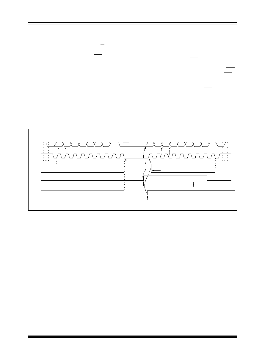
FIGURE 11-20: I2C WAVEFORMS FOR TRANSMISSION (7-BIT ADDRESS)
SDA
SCL
SSPIF (PIR1<3>)
BF (SSPSTAT<0>)
CKP (SSPCON<4>)
A7
A6
A5
A4
A3
A2
A1
ACK
D7
D6
D5
D4
D3
D2
D1
D0
ACK
Transmitting Data
R/W = 1
Receiving Address
1
2
3
4
5
6
7
8
9
1
2
3
4
5
6
7
8
9
P
cleared in software
SSPBUF is written in software
From SSP interrupt
service routine
Set bit after writing to SSPBUF
S
Data in
sampled
SCL held low
while CPU
responds to SSPIF
(the SSPBUF must be written-to
before the CKP bit can be set)
相关PDF资料 |
PDF描述 |
|---|---|
| PIC18F458T-I/PT | IC MCU FLASH 16KX16 W/CAN 44TQFP |
| PIC16LC77-04I/PQ | IC MCU OTP 8KX14 A/D PWM 44-MQFP |
| GRM31MR61C685KA12L | CAP CER 6.8UF 16V 10% X5R 1206 |
| RPER72A333K2P1C03B | CAP CER 0.033UF 100V 10% RADIAL |
| RPER72A333K2K1C03B | CAP CER 0.033UF 100V 10% RADIAL |
相关代理商/技术参数 |
参数描述 |
|---|---|
| PIC18LF4539-I/ML | 功能描述:8位微控制器 -MCU 24KB 1408 RAM 32I/O RoHS:否 制造商:Silicon Labs 核心:8051 处理器系列:C8051F39x 数据总线宽度:8 bit 最大时钟频率:50 MHz 程序存储器大小:16 KB 数据 RAM 大小:1 KB 片上 ADC:Yes 工作电源电压:1.8 V to 3.6 V 工作温度范围:- 40 C to + 105 C 封装 / 箱体:QFN-20 安装风格:SMD/SMT |
| PIC18LF4539-I/P | 功能描述:8位微控制器 -MCU 24KB 1408 RAM 32I/O RoHS:否 制造商:Silicon Labs 核心:8051 处理器系列:C8051F39x 数据总线宽度:8 bit 最大时钟频率:50 MHz 程序存储器大小:16 KB 数据 RAM 大小:1 KB 片上 ADC:Yes 工作电源电压:1.8 V to 3.6 V 工作温度范围:- 40 C to + 105 C 封装 / 箱体:QFN-20 安装风格:SMD/SMT |
| PIC18LF4539-I/PT | 功能描述:8位微控制器 -MCU 24KB 1408 RAM 32I/O RoHS:否 制造商:Silicon Labs 核心:8051 处理器系列:C8051F39x 数据总线宽度:8 bit 最大时钟频率:50 MHz 程序存储器大小:16 KB 数据 RAM 大小:1 KB 片上 ADC:Yes 工作电源电压:1.8 V to 3.6 V 工作温度范围:- 40 C to + 105 C 封装 / 箱体:QFN-20 安装风格:SMD/SMT |
| PIC18LF4539T-I/ML | 功能描述:8位微控制器 -MCU 24KB 1408 RAM 32I/O RoHS:否 制造商:Silicon Labs 核心:8051 处理器系列:C8051F39x 数据总线宽度:8 bit 最大时钟频率:50 MHz 程序存储器大小:16 KB 数据 RAM 大小:1 KB 片上 ADC:Yes 工作电源电压:1.8 V to 3.6 V 工作温度范围:- 40 C to + 105 C 封装 / 箱体:QFN-20 安装风格:SMD/SMT |
| PIC18LF4539T-I/PT | 功能描述:8位微控制器 -MCU 24KB 1408 RAM 32I/O RoHS:否 制造商:Silicon Labs 核心:8051 处理器系列:C8051F39x 数据总线宽度:8 bit 最大时钟频率:50 MHz 程序存储器大小:16 KB 数据 RAM 大小:1 KB 片上 ADC:Yes 工作电源电压:1.8 V to 3.6 V 工作温度范围:- 40 C to + 105 C 封装 / 箱体:QFN-20 安装风格:SMD/SMT |
发布紧急采购,3分钟左右您将得到回复。