- 您现在的位置:买卖IC网 > PDF目录11749 > PIC18LF46K80-I/P (Microchip Technology)MCU PIC ECAN 64KB FLASH 40DIP PDF资料下载
参数资料
| 型号: | PIC18LF46K80-I/P |
| 厂商: | Microchip Technology |
| 文件页数: | 130/351页 |
| 文件大小: | 0K |
| 描述: | MCU PIC ECAN 64KB FLASH 40DIP |
| 产品培训模块: | 8-bit PIC® Microcontroller Portfolio |
| 标准包装: | 10 |
| 系列: | PIC® XLP™ 18F |
| 核心处理器: | PIC |
| 芯体尺寸: | 8-位 |
| 速度: | 64MHz |
| 连通性: | ECAN,I²C,LIN,SPI,UART/USART |
| 外围设备: | 欠压检测/复位,LVD,POR,PWM,WDT |
| 输入/输出数: | 35 |
| 程序存储器容量: | 64KB(32K x 16) |
| 程序存储器类型: | 闪存 |
| EEPROM 大小: | 1K x 8 |
| RAM 容量: | 3.6K x 8 |
| 电压 - 电源 (Vcc/Vdd): | 1.8 V ~ 3.6 V |
| 数据转换器: | A/D 11x12b |
| 振荡器型: | 内部 |
| 工作温度: | -40°C ~ 85°C |
| 封装/外壳: | 40-DIP(0.600",15.24mm) |
| 包装: | 管件 |
第1页第2页第3页第4页第5页第6页第7页第8页第9页第10页第11页第12页第13页第14页第15页第16页第17页第18页第19页第20页第21页第22页第23页第24页第25页第26页第27页第28页第29页第30页第31页第32页第33页第34页第35页第36页第37页第38页第39页第40页第41页第42页第43页第44页第45页第46页第47页第48页第49页第50页第51页第52页第53页第54页第55页第56页第57页第58页第59页第60页第61页第62页第63页第64页第65页第66页第67页第68页第69页第70页第71页第72页第73页第74页第75页第76页第77页第78页第79页第80页第81页第82页第83页第84页第85页第86页第87页第88页第89页第90页第91页第92页第93页第94页第95页第96页第97页第98页第99页第100页第101页第102页第103页第104页第105页第106页第107页第108页第109页第110页第111页第112页第113页第114页第115页第116页第117页第118页第119页第120页第121页第122页第123页第124页第125页第126页第127页第128页第129页当前第130页第131页第132页第133页第134页第135页第136页第137页第138页第139页第140页第141页第142页第143页第144页第145页第146页第147页第148页第149页第150页第151页第152页第153页第154页第155页第156页第157页第158页第159页第160页第161页第162页第163页第164页第165页第166页第167页第168页第169页第170页第171页第172页第173页第174页第175页第176页第177页第178页第179页第180页第181页第182页第183页第184页第185页第186页第187页第188页第189页第190页第191页第192页第193页第194页第195页第196页第197页第198页第199页第200页第201页第202页第203页第204页第205页第206页第207页第208页第209页第210页第211页第212页第213页第214页第215页第216页第217页第218页第219页第220页第221页第222页第223页第224页第225页第226页第227页第228页第229页第230页第231页第232页第233页第234页第235页第236页第237页第238页第239页第240页第241页第242页第243页第244页第245页第246页第247页第248页第249页第250页第251页第252页第253页第254页第255页第256页第257页第258页第259页第260页第261页第262页第263页第264页第265页第266页第267页第268页第269页第270页第271页第272页第273页第274页第275页第276页第277页第278页第279页第280页第281页第282页第283页第284页第285页第286页第287页第288页第289页第290页第291页第292页第293页第294页第295页第296页第297页第298页第299页第300页第301页第302页第303页第304页第305页第306页第307页第308页第309页第310页第311页第312页第313页第314页第315页第316页第317页第318页第319页第320页第321页第322页第323页第324页第325页第326页第327页第328页第329页第330页第331页第332页第333页第334页第335页第336页第337页第338页第339页第340页第341页第342页第343页第344页第345页第346页第347页第348页第349页第350页第351页
2010-2012 Microchip Technology Inc.
DS39977F-page 215
PIC18F66K80 FAMILY
For more details on selecting the optimum C1 and C2
for a given crystal, see the crystal manufacture’s appli-
cations information. The optimum value depends in
part on the amount of parasitic capacitance in the
circuit, which is often unknown. For that reason, it is
highly recommended that thorough testing and valida-
tion of the oscillator be performed after values have
been selected.
14.5.1
USING SOSC AS A
CLOCK SOURCE
The SOSC oscillator is also available as a clock source
in power-managed modes. By setting the clock select
bits, SCS<1:0> (OSCCON<1:0>), to ‘01’, the device
switches to SEC_RUN mode and both the CPU and
peripherals are clocked from the SOSC oscillator. If the
IDLEN bit (OSCCON<7>) is cleared and a SLEEP
instruction is executed, the device enters SEC_IDLE
mode. Additional details are available in Section 4.0
Whenever the SOSC oscillator is providing the clock
source, the SOSC System Clock Status flag,
SOSCRUN (OSCCON2<6>), is set. This can be used
to determine the controller’s current clocking mode. It
can also indicate the clock source currently being used
by the Fail-Safe Clock Monitor.
If the Clock Monitor is enabled and the SOSC oscillator
fails while providing the clock, polling the SOCSRUN
bit will indicate whether the clock is being provided by
the SOSC oscillator or another source.
14.5.2
SOSC OSCILLATOR LAYOUT
CONSIDERATIONS
The SOSC oscillator circuit draws very little power
during operation. Due to the low-power nature of the
oscillator, it may also be sensitive to rapidly changing
signals in close proximity. This is especially true when
the oscillator is configured for extremely Low-Power
mode, SOSCSEL<1:0> (CONFIG1L<4:3>) = 01.
The oscillator circuit, displayed in Figure 14-2, should
be located as close as possible to the microcontroller.
There should be no circuits passing within the oscillator
circuit boundaries other than VSS or VDD.
If a high-speed circuit must be located near the oscillator,
it may help to have a grounded guard ring around the
oscillator circuit. The guard, as displayed in Figure 14-3,
could be used on a single-sided PCB or in addition to a
ground plane. (Examples of a high-speed circuit include
the ECCP1 pin, in Output Compare or PWM mode, or
the primary oscillator, using the OSC2 pin.)
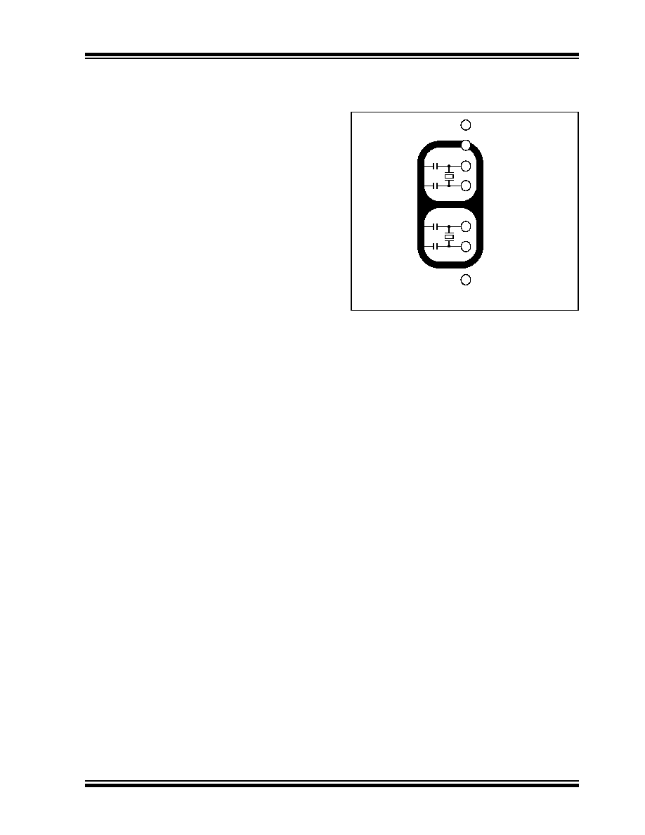
FIGURE 14-3:
OSCILLATOR CIRCUIT
WITH GROUNDED
GUARD RING
In the Low Drive Level mode, SOSCSEL<1:0> = 01, it is
critical that RC2 I/O pin signals be kept away from the
oscillator circuit. Configuring RC2 as a digital output, and
toggling it, can potentially disturb the oscillator circuit,
even with a relatively good PCB layout. If possible, either
leave RC2 unused or use it as an input pin with a slew
rate limited signal source. If RC2 must be used as a
digital output, it may be necessary to use the Higher
Drive Level Oscillator mode (SOSCSEL<1:0> = 11) with
many PCB layouts.
Even in the Higher Drive Level mode, careful layout
procedures should still be followed when designing the
oscillator circuit.
In addition to dV/dt induced noise considerations, it is
important to ensure that the circuit board is clean. Even
a very small amount of conductive, soldering flux
residue can cause PCB leakage currents that can
overwhelm the oscillator circuit.
14.6
Timer1 Interrupt
The TMR1 register pair (TMR1H:TMR1L) increments
from 0000h to FFFFh and rolls over to 0000h. The
Timer1 interrupt, if enabled, is generated on overflow
which is latched in interrupt flag bit, TMR1IF
(PIR1<0>). This interrupt can be enabled or disabled
by setting or clearing the Timer1 Interrupt Enable bit,
TMR1IE (PIE1<0>).
VDD
OSC1
VSS
OSC2
RC0
RC1
RC2
Note:
Not drawn to scale.
相关PDF资料 |
PDF描述 |
|---|---|
| MS27468E13B22S | CONN RCPT 22POS JAM NUT W/SCKT |
| VE-B4F-IW-F1 | CONVERTER MOD DC/DC 72V 100W |
| PIC16LC620-04/SO | IC MCU OTP 512X14 COMP 18SOIC |
| VE-B4D-IX-F4 | CONVERTER MOD DC/DC 85V 75W |
| PIC16LC621-04/P | IC MCU OTP 1KX14 COMP 18DIP |
相关代理商/技术参数 |
参数描述 |
|---|---|
| PIC18LF46K80T-I/ML | 功能描述:8位微控制器 -MCU 64KB FL 4KBRM 16MIPS 12bit ADC CTMU XLP RoHS:否 制造商:Silicon Labs 核心:8051 处理器系列:C8051F39x 数据总线宽度:8 bit 最大时钟频率:50 MHz 程序存储器大小:16 KB 数据 RAM 大小:1 KB 片上 ADC:Yes 工作电源电压:1.8 V to 3.6 V 工作温度范围:- 40 C to + 105 C 封装 / 箱体:QFN-20 安装风格:SMD/SMT |
| PIC18LF46K80T-I/PT | 功能描述:8位微控制器 -MCU 64KB FL 4KBRM 16MIPS 12bit ADC CTMU XLP RoHS:否 制造商:Silicon Labs 核心:8051 处理器系列:C8051F39x 数据总线宽度:8 bit 最大时钟频率:50 MHz 程序存储器大小:16 KB 数据 RAM 大小:1 KB 片上 ADC:Yes 工作电源电压:1.8 V to 3.6 V 工作温度范围:- 40 C to + 105 C 封装 / 箱体:QFN-20 安装风格:SMD/SMT |
| PIC18LF47J13-I/ML | 功能描述:8位微控制器 -MCU 128KB Flash 4KB RAM 12MIPS nanoWatt RoHS:否 制造商:Silicon Labs 核心:8051 处理器系列:C8051F39x 数据总线宽度:8 bit 最大时钟频率:50 MHz 程序存储器大小:16 KB 数据 RAM 大小:1 KB 片上 ADC:Yes 工作电源电压:1.8 V to 3.6 V 工作温度范围:- 40 C to + 105 C 封装 / 箱体:QFN-20 安装风格:SMD/SMT |
| PIC18LF47J13-I/PT | 功能描述:8位微控制器 -MCU 128KB Flash 4KB RAM 12MIPS nanoWatt RoHS:否 制造商:Silicon Labs 核心:8051 处理器系列:C8051F39x 数据总线宽度:8 bit 最大时钟频率:50 MHz 程序存储器大小:16 KB 数据 RAM 大小:1 KB 片上 ADC:Yes 工作电源电压:1.8 V to 3.6 V 工作温度范围:- 40 C to + 105 C 封装 / 箱体:QFN-20 安装风格:SMD/SMT |
| PIC18LF47J13T-I/ML | 功能描述:8位微控制器 -MCU GP 128KB Flash 4KB RAM 12 MIPS 12b ADC RoHS:否 制造商:Silicon Labs 核心:8051 处理器系列:C8051F39x 数据总线宽度:8 bit 最大时钟频率:50 MHz 程序存储器大小:16 KB 数据 RAM 大小:1 KB 片上 ADC:Yes 工作电源电压:1.8 V to 3.6 V 工作温度范围:- 40 C to + 105 C 封装 / 箱体:QFN-20 安装风格:SMD/SMT |
发布紧急采购,3分钟左右您将得到回复。