- 您现在的位置:买卖IC网 > PDF目录11749 > PIC18LF47J13-I/PT (Microchip Technology)IC PIC MCU 128KB FLASH 44TQFP PDF资料下载
参数资料
| 型号: | PIC18LF47J13-I/PT |
| 厂商: | Microchip Technology |
| 文件页数: | 28/71页 |
| 文件大小: | 0K |
| 描述: | IC PIC MCU 128KB FLASH 44TQFP |
| 产品培训模块: | 8-bit PIC® Microcontroller Portfolio |
| 标准包装: | 160 |
| 系列: | PIC® XLP™ 18F |
| 核心处理器: | PIC |
| 芯体尺寸: | 8-位 |
| 速度: | 48MHz |
| 连通性: | I²C,LIN,SPI,UART/USART |
| 外围设备: | 欠压检测/复位,POR,PWM,WDT |
| 输入/输出数: | 34 |
| 程序存储器容量: | 128KB(64K x 16) |
| 程序存储器类型: | 闪存 |
| RAM 容量: | 3.8K x 8 |
| 电压 - 电源 (Vcc/Vdd): | 2 V ~ 2.75 V |
| 数据转换器: | A/D 13x10b/12b |
| 振荡器型: | 内部 |
| 工作温度: | -40°C ~ 85°C |
| 封装/外壳: | 44-TQFP |
| 包装: | 管件 |
第1页第2页第3页第4页第5页第6页第7页第8页第9页第10页第11页第12页第13页第14页第15页第16页第17页第18页第19页第20页第21页第22页第23页第24页第25页第26页第27页当前第28页第29页第30页第31页第32页第33页第34页第35页第36页第37页第38页第39页第40页第41页第42页第43页第44页第45页第46页第47页第48页第49页第50页第51页第52页第53页第54页第55页第56页第57页第58页第59页第60页第61页第62页第63页第64页第65页第66页第67页第68页第69页第70页第71页
PIC18(L)F2X/4XK22
DS41412E-page 34
2010-2012 Microchip Technology Inc.
2.4
Clock Source Modes
Clock Source modes can be classified as external or
internal.
External Clock modes rely on external circuitry for
the clock source. Examples are: Clock modules
(EC mode), quartz crystal resonators or ceramic
resonators (LP, XT and HS modes) and Resistor-
Capacitor (RC mode) circuits.
Internal clock sources are contained internally
within the Oscillator block. The Oscillator block
has three internal oscillators: the 16 MHz High-
Frequency Internal Oscillator (HFINTOSC),
500 kHz Medium-Frequency Internal Oscillator
(MFINTOSC) and the 31.25 kHz Low-Frequency
Internal Oscillator (LFINTOSC).
The system clock can be selected between external or
internal clock sources via the System Clock Select
(SCS<1:0>) bits of the OSCCON register. See
for
additional
information.
2.5
External Clock Modes
2.5.1
OSCILLATOR START-UP TIMER (OST)
When the oscillator module is configured for LP, XT or
HS modes, the Oscillator Start-up Timer (OST) counts
1024 oscillations from OSC1. This occurs following a
Power-on Reset (POR) and when the Power-up Timer
(PWRT) has expired (if configured), or a wake-up from
Sleep. During this time, the program counter does not
increment and program execution is suspended. The
OST ensures that the oscillator circuit, using a quartz
crystal resonator or ceramic resonator, has started and
is providing a stable system clock to the oscillator
module. When switching between clock sources, a
delay is required to allow the new clock to stabilize.
These oscillator delays are shown in Table 2-2.
In order to minimize latency between external oscillator
start-up and code execution, the Two-Speed Clock
Start-up mode can be selected (see Section 2.12
TABLE 2-2:
OSCILLATOR DELAY EXAMPLES
2.5.2
EC MODE
The External Clock (EC) mode allows an externally
generated logic level as the system clock source. When
operating in this mode, an external clock source is
connected to the OSC1 input and the OSC2 is available
for general purpose I/O. Figure 2-5 shows the pin
connections for EC mode.
The External Clock (EC) offers different power modes,
Low Power (ECLP), Medium Power (ECMP) and High
Power (ECHP), selectable by the FOSC<3:0> bits.
Each mode is best suited for a certain range of
frequencies. The ranges are:
ECLP – below 500 kHz
ECMP – between 500 kHz and 16 MHz
ECHP – above 16 MHz
The Oscillator Start-up Timer (OST) is disabled when
EC mode is selected. Therefore, there is no delay in
operation after a Power-on Reset (POR) or wake-up
from Sleep. Because the PIC MCU design is fully
static, stopping the external clock input will have the
effect of halting the device while leaving all data intact.
Upon restarting the external clock, the device will
resume operation as if no time had elapsed.
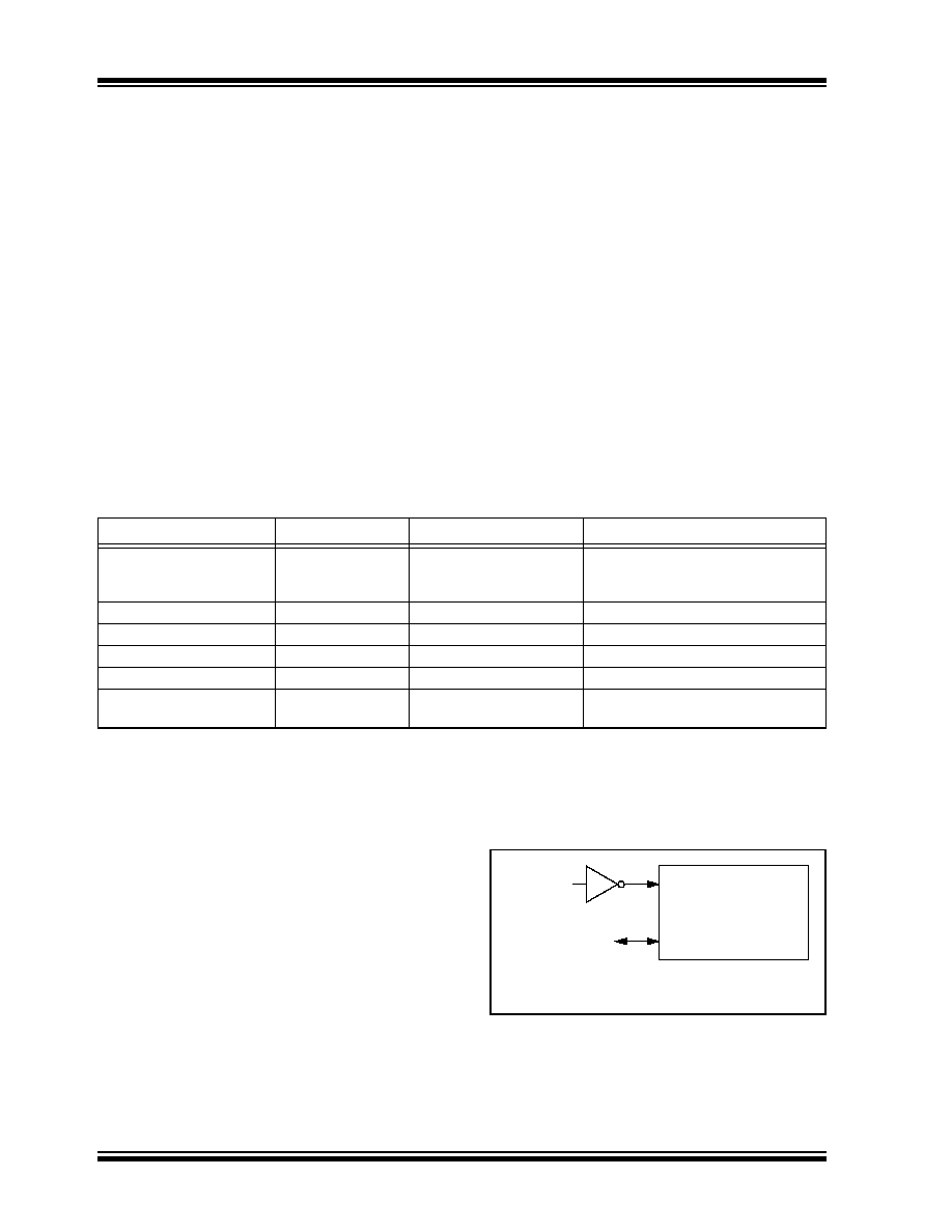
FIGURE 2-5:
EXTERNAL CLOCK (EC)
MODE OPERATION
Switch From
Switch To
Frequency
Oscillator Delay
Sleep/POR
LFINTOSC
MFINTOSC
HFINTOSC
31.25 kHz
31.25 kHz to 500 kHz
31.25 kHz to 16 MHz
Oscillator Warm-Up Delay (TWARM)
Sleep/POR
EC, RC
DC – 64 MHz
2 instruction cycles
LFINTOSC (31.25 kHz)
EC, RC
DC – 64 MHz
1 cycle of each
Sleep/POR
LP, XT, HS
32 kHz to 40 MHz
1024 Clock Cycles (OST)
Sleep/POR
4xPLL
32 MHz to 64 MHz
1024 Clock Cycles (OST) + 2 ms
LFINTOSC (31.25 kHz)
LFINTOSC
HFINTOSC
31.25 kHz to 16 MHz
1
s (approx.)
OSC1/CLKIN
OSC2/CLKOUT(1)
I/O
Clock from
Ext. System
PIC MCU
Note
1:
Alternate pin functions are listed in
相关PDF资料 |
PDF描述 |
|---|---|
| DSPIC33FJ32GP202-I/MM | IC DSPIC MCU/DSP 32K 28QFN |
| VE-B4H-IW-F3 | CONVERTER MOD DC/DC 52V 100W |
| CE2S101C02 | COAX BOARD SIDE CONNECTOR |
| VE-B4H-IW-F2 | CONVERTER MOD DC/DC 52V 100W |
| VE-B4F-IW-F4 | CONVERTER MOD DC/DC 72V 100W |
相关代理商/技术参数 |
参数描述 |
|---|---|
| PIC18LF47J13T-I/ML | 功能描述:8位微控制器 -MCU GP 128KB Flash 4KB RAM 12 MIPS 12b ADC RoHS:否 制造商:Silicon Labs 核心:8051 处理器系列:C8051F39x 数据总线宽度:8 bit 最大时钟频率:50 MHz 程序存储器大小:16 KB 数据 RAM 大小:1 KB 片上 ADC:Yes 工作电源电压:1.8 V to 3.6 V 工作温度范围:- 40 C to + 105 C 封装 / 箱体:QFN-20 安装风格:SMD/SMT |
| PIC18LF47J13T-I/PT | 功能描述:8位微控制器 -MCU GP 128KB Flash 4KB RAM 12 MIPS 12b ADC RoHS:否 制造商:Silicon Labs 核心:8051 处理器系列:C8051F39x 数据总线宽度:8 bit 最大时钟频率:50 MHz 程序存储器大小:16 KB 数据 RAM 大小:1 KB 片上 ADC:Yes 工作电源电压:1.8 V to 3.6 V 工作温度范围:- 40 C to + 105 C 封装 / 箱体:QFN-20 安装风格:SMD/SMT |
| PIC18LF47J53-I/ML | 功能描述:8位微控制器 -MCU 128KB Flash 4KB RAM 12MIPS nanoWatt RoHS:否 制造商:Silicon Labs 核心:8051 处理器系列:C8051F39x 数据总线宽度:8 bit 最大时钟频率:50 MHz 程序存储器大小:16 KB 数据 RAM 大小:1 KB 片上 ADC:Yes 工作电源电压:1.8 V to 3.6 V 工作温度范围:- 40 C to + 105 C 封装 / 箱体:QFN-20 安装风格:SMD/SMT |
| PIC18LF47J53-I/PT | 功能描述:8位微控制器 -MCU 128KB Flash 4KB RAM 12MIPS nanoWatt RoHS:否 制造商:Silicon Labs 核心:8051 处理器系列:C8051F39x 数据总线宽度:8 bit 最大时钟频率:50 MHz 程序存储器大小:16 KB 数据 RAM 大小:1 KB 片上 ADC:Yes 工作电源电压:1.8 V to 3.6 V 工作温度范围:- 40 C to + 105 C 封装 / 箱体:QFN-20 安装风格:SMD/SMT |
| PIC18LF47J53T-I/ML | 功能描述:8位微控制器 -MCU USB 128KB Flash 4KB RAM 12 MIPS 12b ADC RoHS:否 制造商:Silicon Labs 核心:8051 处理器系列:C8051F39x 数据总线宽度:8 bit 最大时钟频率:50 MHz 程序存储器大小:16 KB 数据 RAM 大小:1 KB 片上 ADC:Yes 工作电源电压:1.8 V to 3.6 V 工作温度范围:- 40 C to + 105 C 封装 / 箱体:QFN-20 安装风格:SMD/SMT |
发布紧急采购,3分钟左右您将得到回复。