- 您现在的位置:买卖IC网 > PDF目录11411 > PIC18LF6393-I/PT (Microchip Technology)IC PIC MCU FLASH 4KX16 64TQFP PDF资料下载
参数资料
| 型号: | PIC18LF6393-I/PT |
| 厂商: | Microchip Technology |
| 文件页数: | 29/41页 |
| 文件大小: | 0K |
| 描述: | IC PIC MCU FLASH 4KX16 64TQFP |
| 标准包装: | 160 |
| 系列: | PIC® 18F |
| 核心处理器: | PIC |
| 芯体尺寸: | 8-位 |
| 速度: | 40MHz |
| 连通性: | I²C,SPI,UART/USART |
| 外围设备: | 欠压检测/复位,HLVD,LCD,POR,PWM,WDT |
| 输入/输出数: | 50 |
| 程序存储器容量: | 8KB(4K x 16) |
| 程序存储器类型: | 闪存 |
| RAM 容量: | 768 x 8 |
| 电压 - 电源 (Vcc/Vdd): | 2 V ~ 5.5 V |
| 数据转换器: | A/D 12x12b |
| 振荡器型: | 内部 |
| 工作温度: | -40°C ~ 85°C |
| 封装/外壳: | 64-TQFP |
| 包装: | 托盘 |
| 产品目录页面: | 642 (CN2011-ZH PDF) |
第1页第2页第3页第4页第5页第6页第7页第8页第9页第10页第11页第12页第13页第14页第15页第16页第17页第18页第19页第20页第21页第22页第23页第24页第25页第26页第27页第28页当前第29页第30页第31页第32页第33页第34页第35页第36页第37页第38页第39页第40页第41页
2010 Microchip Technology Inc.
DS39896C-page 35
PIC18F6393/6493/8393/8493
The value in the ADRESH:ADRESL registers is
unknown following Power-on and Brown-out Resets and
is not affected by any other Reset.
After the A/D module has been configured as desired,
the selected channel must be acquired before the
conversion is started. The analog input channels must
have their corresponding TRIS bits selected as an
input. To determine acquisition time, see Section 2.1
“A/D Acquisition Requirements”. After this acquisi-
tion time has elapsed, the A/D conversion can be
started. An acquisition time can be programmed to
occur between setting the GO/DONE bit and the actual
start of the conversion.
The following steps should be followed to perform an A/D
conversion:
1.
Configure the A/D module:
Configure analog pins, voltage reference and
digital I/O (ADCON1)
Select A/D input channel (ADCON0)
Select A/D acquisition time (ADCON2)
Select A/D conversion clock (ADCON2)
Turn on A/D module (ADCON0)
2.
Configure A/D interrupt (if desired):
Clear ADIF bit
Set ADIE bit
Set GIE bit
3.
Wait the required acquisition time (if required).
4.
Start conversion:
Set GO/DONE bit (ADCON0<1>)
5.
Wait for A/D conversion to complete by either:
Polling for the GO/DONE bit to be cleared
OR
Waiting for the A/D interrupt
6.
Read A/D Result registers (ADRESH:ADRESL);
clear bit, ADIF, if required.
7.
For the next conversion, go to Step 1 or Step 2,
as required. The A/D conversion time per bit is
defined as TAD. A minimum wait of 2 TAD is
required before the next acquisition starts.
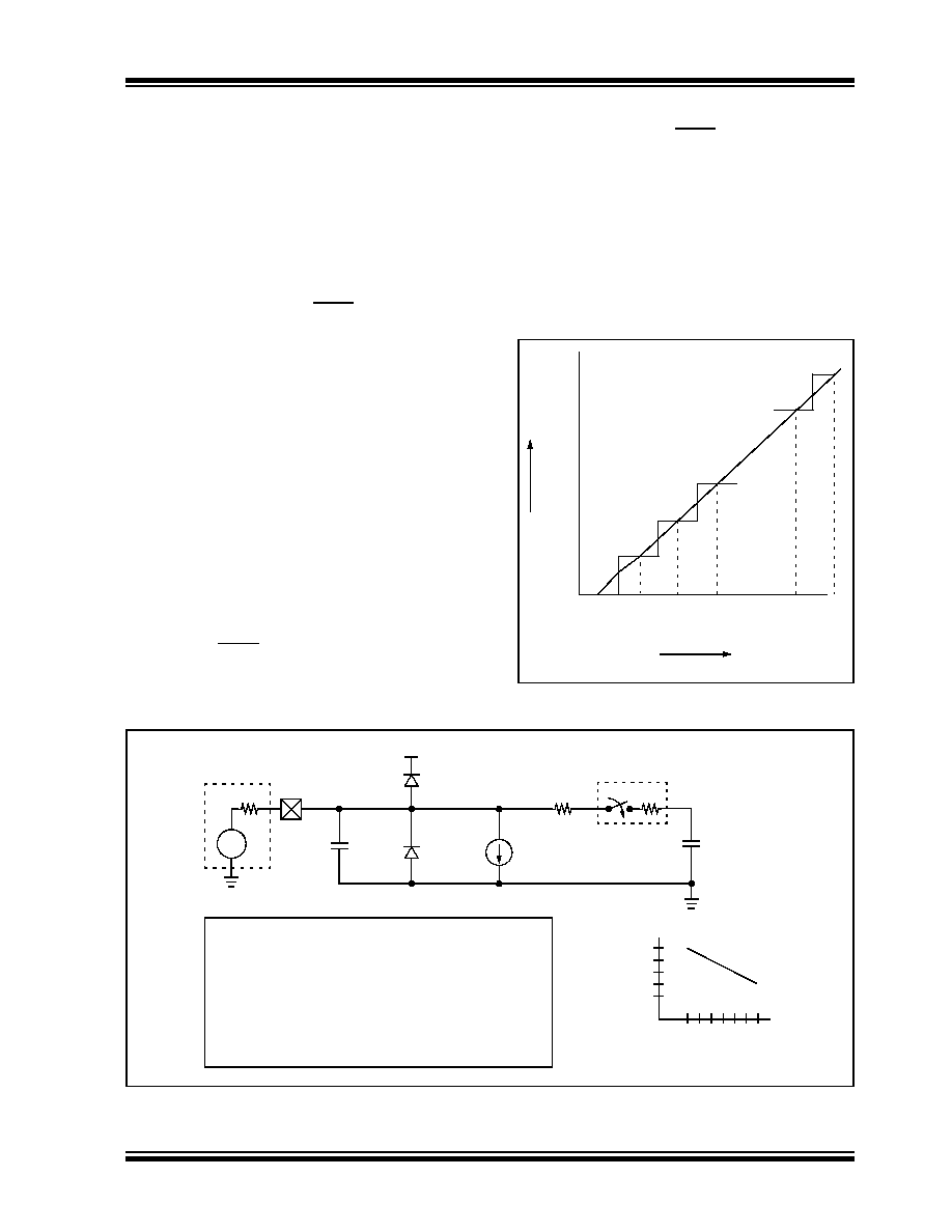
FIGURE 2-2:
A/D TRANSFER FUNCTION
FIGURE 2-3:
ANALOG INPUT MODEL
Dig
ita
lCo
de
Ou
tp
u
t
FFEh
003h
002h
001h
000h
0.
5L
S
B
1L
S
B
1.
5L
S
B
2L
S
B
2.
5L
S
B
40
94
LS
B
40
94.
5L
S
B
3L
S
B
Analog Input Voltage
FFFh
40
95
LS
B
40
95.
5L
S
B
VAIN
CPIN
Rs
ANx
5 pF
VT = 0.6V
ILEAKAGE
RIC
1k
Sampling
Switch
SS
RSS
CHOLD = 25 pF
VSS
VDD
±100 nA
Legend: CPIN
VT
ILEAKAGE
RIC
SS
CHOLD
= Input Capacitance
= Threshold Voltage
= Leakage Current at the pin due to
= Interconnect Resistance
= Sampling Switch
= Sample/Hold Capacitance (from DAC)
various junctions
= Sampling Switch Resistance
RSS
VDD
6V
Sampling Switch
5V
4V
3V
2V
12
3
4
(k
)
相关PDF资料 |
PDF描述 |
|---|---|
| VI-2NN-CV-F3 | CONVERTER MOD DC/DC 18.5V 150W |
| VE-2N2-IY | CONVERTER MOD DC/DC 15V 50W |
| VE-2N2-EU-B1 | CONVERTER MOD DC/DC 15V 200W |
| VE-2N1-IY | CONVERTER MOD DC/DC 12V 50W |
| VE-2N1-EU-B1 | CONVERTER MOD DC/DC 12V 200W |
相关代理商/技术参数 |
参数描述 |
|---|---|
| PIC18LF6393T-I/PT | 功能描述:8位微控制器 -MCU 128 Segmnt LCD DRVR 12B ADC 8KB 768BRAM RoHS:否 制造商:Silicon Labs 核心:8051 处理器系列:C8051F39x 数据总线宽度:8 bit 最大时钟频率:50 MHz 程序存储器大小:16 KB 数据 RAM 大小:1 KB 片上 ADC:Yes 工作电源电压:1.8 V to 3.6 V 工作温度范围:- 40 C to + 105 C 封装 / 箱体:QFN-20 安装风格:SMD/SMT |
| PIC18LF6410-I/PT | 功能描述:8位微控制器 -MCU 16kBF 768RM 68 I/O RoHS:否 制造商:Silicon Labs 核心:8051 处理器系列:C8051F39x 数据总线宽度:8 bit 最大时钟频率:50 MHz 程序存储器大小:16 KB 数据 RAM 大小:1 KB 片上 ADC:Yes 工作电源电压:1.8 V to 3.6 V 工作温度范围:- 40 C to + 105 C 封装 / 箱体:QFN-20 安装风格:SMD/SMT |
| PIC18LF6410T-I/PT | 功能描述:8位微控制器 -MCU 16 KB FL 768 RAM 68 I/O RoHS:否 制造商:Silicon Labs 核心:8051 处理器系列:C8051F39x 数据总线宽度:8 bit 最大时钟频率:50 MHz 程序存储器大小:16 KB 数据 RAM 大小:1 KB 片上 ADC:Yes 工作电源电压:1.8 V to 3.6 V 工作温度范围:- 40 C to + 105 C 封装 / 箱体:QFN-20 安装风格:SMD/SMT |
| PIC18LF6490-I/PT | 功能描述:8位微控制器 -MCU 16kBF 768RM 68 I/O RoHS:否 制造商:Silicon Labs 核心:8051 处理器系列:C8051F39x 数据总线宽度:8 bit 最大时钟频率:50 MHz 程序存储器大小:16 KB 数据 RAM 大小:1 KB 片上 ADC:Yes 工作电源电压:1.8 V to 3.6 V 工作温度范围:- 40 C to + 105 C 封装 / 箱体:QFN-20 安装风格:SMD/SMT |
| PIC18LF6490T-I/PT | 功能描述:8位微控制器 -MCU 16 KB FL 768 RAM 68 I/O RoHS:否 制造商:Silicon Labs 核心:8051 处理器系列:C8051F39x 数据总线宽度:8 bit 最大时钟频率:50 MHz 程序存储器大小:16 KB 数据 RAM 大小:1 KB 片上 ADC:Yes 工作电源电压:1.8 V to 3.6 V 工作温度范围:- 40 C to + 105 C 封装 / 箱体:QFN-20 安装风格:SMD/SMT |
发布紧急采购,3分钟左右您将得到回复。