- 您现在的位置:买卖IC网 > PDF目录11242 > PIC18LF6720T-I/PT (Microchip Technology)IC MCU FLASH 64KX16 LV 64-TQFP PDF资料下载
参数资料
| 型号: | PIC18LF6720T-I/PT |
| 厂商: | Microchip Technology |
| 文件页数: | 87/165页 |
| 文件大小: | 0K |
| 描述: | IC MCU FLASH 64KX16 LV 64-TQFP |
| 产品培训模块: | Asynchronous Stimulus |
| 标准包装: | 1,200 |
| 系列: | PIC® 18F |
| 核心处理器: | PIC |
| 芯体尺寸: | 8-位 |
| 速度: | 25MHz |
| 连通性: | I²C,SPI,UART/USART |
| 外围设备: | 欠压检测/复位,LVD,POR,PWM,WDT |
| 输入/输出数: | 52 |
| 程序存储器容量: | 128KB(64K x 16) |
| 程序存储器类型: | 闪存 |
| EEPROM 大小: | 1K x 8 |
| RAM 容量: | 3.75K x 8 |
| 电压 - 电源 (Vcc/Vdd): | 2 V ~ 5.5 V |
| 数据转换器: | A/D 12x10b |
| 振荡器型: | 外部 |
| 工作温度: | -40°C ~ 85°C |
| 封装/外壳: | 64-TQFP |
| 包装: | 带卷 (TR) |
第1页第2页第3页第4页第5页第6页第7页第8页第9页第10页第11页第12页第13页第14页第15页第16页第17页第18页第19页第20页第21页第22页第23页第24页第25页第26页第27页第28页第29页第30页第31页第32页第33页第34页第35页第36页第37页第38页第39页第40页第41页第42页第43页第44页第45页第46页第47页第48页第49页第50页第51页第52页第53页第54页第55页第56页第57页第58页第59页第60页第61页第62页第63页第64页第65页第66页第67页第68页第69页第70页第71页第72页第73页第74页第75页第76页第77页第78页第79页第80页第81页第82页第83页第84页第85页第86页当前第87页第88页第89页第90页第91页第92页第93页第94页第95页第96页第97页第98页第99页第100页第101页第102页第103页第104页第105页第106页第107页第108页第109页第110页第111页第112页第113页第114页第115页第116页第117页第118页第119页第120页第121页第122页第123页第124页第125页第126页第127页第128页第129页第130页第131页第132页第133页第134页第135页第136页第137页第138页第139页第140页第141页第142页第143页第144页第145页第146页第147页第148页第149页第150页第151页第152页第153页第154页第155页第156页第157页第158页第159页第160页第161页第162页第163页第164页第165页
PIC18F6520/8520/6620/8620/6720/8720
DS39609B-page 26
2004 Microchip Technology Inc.
2.6.2
OSCILLATOR TRANSITIONS
PIC18FXX20 devices contain circuitry to prevent
“glitches” when switching between oscillator sources.
Essentially, the circuitry waits for eight rising edges of
the clock source that the processor is switching to. This
ensures that the new clock source is stable and that its
pulse width will not be less than the shortest pulse
width of the two clock sources.
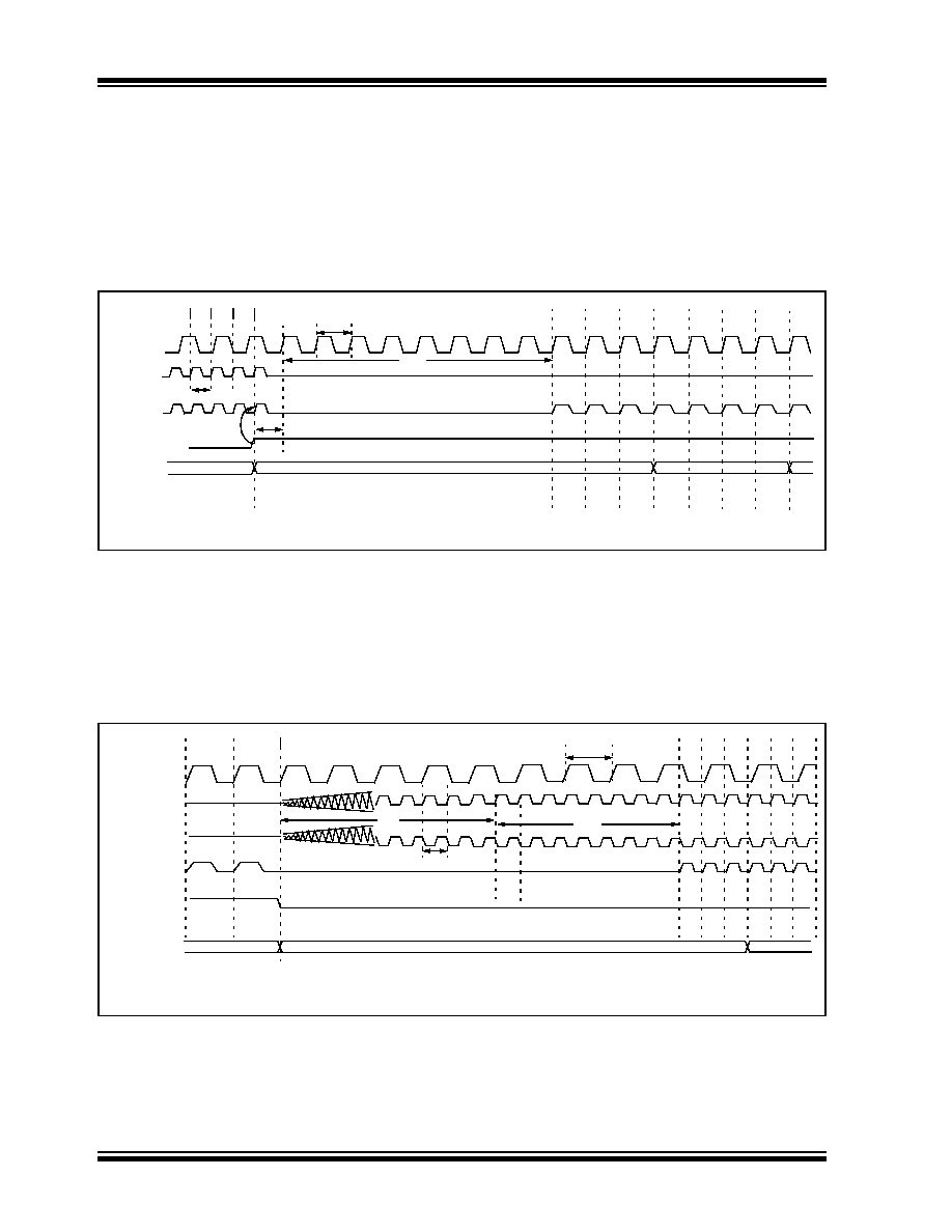
A timing diagram indicating the transition from the main
oscillator to the Timer1 oscillator is shown in Figure 2-8.
The Timer1 oscillator is assumed to be running all the
time. After the SCS bit is set, the processor is frozen at
the next occurring Q1 cycle. After eight synchronization
cycles are counted from the Timer1 oscillator, operation
resumes. No additional delays are required after the
synchronization cycles.
FIGURE 2-8:
TIMING DIAGRAM FOR TRANSITION FROM OSC1 TO TIMER1 OSCILLATOR
The sequence of events that takes place when switch-
ing from the Timer1 oscillator to the main oscillator will
depend on the mode of the main oscillator. In addition
to eight clock cycles of the main oscillator, additional
delays may take place.
If the main oscillator is configured for an external
crystal (HS, XT, LP), then the transition will take place
after an oscillator start-up time (TOST) has occurred. A
timing diagram, indicating the transition from the
Timer1 oscillator to the main oscillator for HS, XT and
LP modes, is shown in Figure 2-9.
FIGURE 2-9:
TIMING FOR TRANSITION BETWEEN TIMER1 AND OSC1 (HS, XT, LP)
Q3
Q2
Q1
Q4
Q3
Q2
OSC1
Internal
SCS
(OSCCON<0>)
Program
PC + 2
PC
Note 1: Delay on internal system clock is eight oscillator cycles for synchronization.
Q1
T1OSI
Q4
Q1
PC + 4
Q1
TSCS
Clock
Counter
System
Q2
Q3
Q4
Q1
TDLY
TT1P
TOSC
2
1
3
4
5678
Q3
Q4
Q1
Q2
Q3
Q4
Q1
Q2
OSC1
Internal
SCS
(OSCCON<0>)
Program
PC
PC + 2
Note 1: TOST = 1024 TOSC (drawing not to scale).
T1OSI
System Clock
OSC2
TOST
Q1
PC + 6
TT1P
TOSC
TSCS
12
3
4
5
6
7
8
Counter
相关PDF资料 |
PDF描述 |
|---|---|
| ADG708BRU-REEL7 | IC MULTIPLEXER 8X1 16TSSOP |
| ADG736BRM | IC SWITCH DUAL SPDT 10MSOP |
| VE-B3J-IY-S | CONVERTER MOD DC/DC 36V 50W |
| ADG709CRUZ-REEL | IC MULTIPLEXER DUAL 4X1 16TSSOP |
| PIC17LC44-08I/PQ | IC MCU OTP 8KX16 PWM 44-MQFP |
相关代理商/技术参数 |
参数描述 |
|---|---|
| PIC18LF6721-I/PT | 功能描述:8位微控制器 -MCU 128kBF 4096RM 40MHz nonoWatt RoHS:否 制造商:Silicon Labs 核心:8051 处理器系列:C8051F39x 数据总线宽度:8 bit 最大时钟频率:50 MHz 程序存储器大小:16 KB 数据 RAM 大小:1 KB 片上 ADC:Yes 工作电源电压:1.8 V to 3.6 V 工作温度范围:- 40 C to + 105 C 封装 / 箱体:QFN-20 安装风格:SMD/SMT |
| PIC18LF6721T-I/PT | 功能描述:8位微控制器 -MCU 128kBF 4096RM 40MHz nonoWatt RoHS:否 制造商:Silicon Labs 核心:8051 处理器系列:C8051F39x 数据总线宽度:8 bit 最大时钟频率:50 MHz 程序存储器大小:16 KB 数据 RAM 大小:1 KB 片上 ADC:Yes 工作电源电压:1.8 V to 3.6 V 工作温度范围:- 40 C to + 105 C 封装 / 箱体:QFN-20 安装风格:SMD/SMT |
| PIC18LF6722-I/PT | 功能描述:8位微控制器 -MCU 128 KB FL 4K RAM 70 I/O RoHS:否 制造商:Silicon Labs 核心:8051 处理器系列:C8051F39x 数据总线宽度:8 bit 最大时钟频率:50 MHz 程序存储器大小:16 KB 数据 RAM 大小:1 KB 片上 ADC:Yes 工作电源电压:1.8 V to 3.6 V 工作温度范围:- 40 C to + 105 C 封装 / 箱体:QFN-20 安装风格:SMD/SMT |
| PIC18LF6722-I/PT | 制造商:Microchip Technology Inc 功能描述:8-Bit Microcontroller IC |
| PIC18LF6722T-I/PT | 功能描述:8位微控制器 -MCU 128 KB FL 4K RAM 70 I/O RoHS:否 制造商:Silicon Labs 核心:8051 处理器系列:C8051F39x 数据总线宽度:8 bit 最大时钟频率:50 MHz 程序存储器大小:16 KB 数据 RAM 大小:1 KB 片上 ADC:Yes 工作电源电压:1.8 V to 3.6 V 工作温度范围:- 40 C to + 105 C 封装 / 箱体:QFN-20 安装风格:SMD/SMT |
发布紧急采购,3分钟左右您将得到回复。