- 您现在的位置:买卖IC网 > PDF目录1965 > PIC18LF8621-I/PT (Microchip Technology)IC PIC MCU FLASH 32KX16 80TQFP PDF资料下载
参数资料
| 型号: | PIC18LF8621-I/PT |
| 厂商: | Microchip Technology |
| 文件页数: | 41/396页 |
| 文件大小: | 0K |
| 描述: | IC PIC MCU FLASH 32KX16 80TQFP |
| 产品培训模块: | Asynchronous Stimulus 8-bit PIC® Microcontroller Portfolio |
| 标准包装: | 119 |
| 系列: | PIC® 18F |
| 核心处理器: | PIC |
| 芯体尺寸: | 8-位 |
| 速度: | 40MHz |
| 连通性: | EBI/EMI,I²C,SPI,UART/USART |
| 外围设备: | 欠压检测/复位,LVD,POR,PWM,WDT |
| 输入/输出数: | 69 |
| 程序存储器容量: | 64KB(32K x 16) |
| 程序存储器类型: | 闪存 |
| EEPROM 大小: | 1K x 8 |
| RAM 容量: | 3.8K x 8 |
| 电压 - 电源 (Vcc/Vdd): | 2 V ~ 5.5 V |
| 数据转换器: | A/D 16x10b |
| 振荡器型: | 外部 |
| 工作温度: | -40°C ~ 85°C |
| 封装/外壳: | 80-TQFP |
| 包装: | 托盘 |
第1页第2页第3页第4页第5页第6页第7页第8页第9页第10页第11页第12页第13页第14页第15页第16页第17页第18页第19页第20页第21页第22页第23页第24页第25页第26页第27页第28页第29页第30页第31页第32页第33页第34页第35页第36页第37页第38页第39页第40页当前第41页第42页第43页第44页第45页第46页第47页第48页第49页第50页第51页第52页第53页第54页第55页第56页第57页第58页第59页第60页第61页第62页第63页第64页第65页第66页第67页第68页第69页第70页第71页第72页第73页第74页第75页第76页第77页第78页第79页第80页第81页第82页第83页第84页第85页第86页第87页第88页第89页第90页第91页第92页第93页第94页第95页第96页第97页第98页第99页第100页第101页第102页第103页第104页第105页第106页第107页第108页第109页第110页第111页第112页第113页第114页第115页第116页第117页第118页第119页第120页第121页第122页第123页第124页第125页第126页第127页第128页第129页第130页第131页第132页第133页第134页第135页第136页第137页第138页第139页第140页第141页第142页第143页第144页第145页第146页第147页第148页第149页第150页第151页第152页第153页第154页第155页第156页第157页第158页第159页第160页第161页第162页第163页第164页第165页第166页第167页第168页第169页第170页第171页第172页第173页第174页第175页第176页第177页第178页第179页第180页第181页第182页第183页第184页第185页第186页第187页第188页第189页第190页第191页第192页第193页第194页第195页第196页第197页第198页第199页第200页第201页第202页第203页第204页第205页第206页第207页第208页第209页第210页第211页第212页第213页第214页第215页第216页第217页第218页第219页第220页第221页第222页第223页第224页第225页第226页第227页第228页第229页第230页第231页第232页第233页第234页第235页第236页第237页第238页第239页第240页第241页第242页第243页第244页第245页第246页第247页第248页第249页第250页第251页第252页第253页第254页第255页第256页第257页第258页第259页第260页第261页第262页第263页第264页第265页第266页第267页第268页第269页第270页第271页第272页第273页第274页第275页第276页第277页第278页第279页第280页第281页第282页第283页第284页第285页第286页第287页第288页第289页第290页第291页第292页第293页第294页第295页第296页第297页第298页第299页第300页第301页第302页第303页第304页第305页第306页第307页第308页第309页第310页第311页第312页第313页第314页第315页第316页第317页第318页第319页第320页第321页第322页第323页第324页第325页第326页第327页第328页第329页第330页第331页第332页第333页第334页第335页第336页第337页第338页第339页第340页第341页第342页第343页第344页第345页第346页第347页第348页第349页第350页第351页第352页第353页第354页第355页第356页第357页第358页第359页第360页第361页第362页第363页第364页第365页第366页第367页第368页第369页第370页第371页第372页第373页第374页第375页第376页第377页第378页第379页第380页第381页第382页第383页第384页第385页第386页第387页第388页第389页第390页第391页第392页第393页第394页第395页第396页
2005 Microchip Technology Inc.
DS39612B-page 133
PIC18F6525/6621/8525/8621
11.1
Timer0 Operation
Timer0 can operate as a timer or as a counter.
Timer mode is selected by clearing the T0CS bit. In
Timer mode, the Timer0 module will increment every
instruction cycle (without prescaler). If the TMR0 regis-
ter is written, the increment is inhibited for the following
two instruction cycles. The user can work around this
by writing an adjusted value to the TMR0 register.
Counter mode is selected by setting the T0CS bit. In
Counter mode, Timer0 will increment, either on every
rising or falling edge of pin RA4/T0CKI. The increment-
ing edge is determined by the Timer0 Source Edge
Select bit (T0SE). Clearing the T0SE bit selects the
rising edge. Restrictions on the external clock input are
discussed below.
When an external clock input is used for Timer0, it must
meet certain requirements. The requirements ensure
the external clock can be synchronized with the internal
phase clock (TOSC). Also, there is a delay in the actual
incrementing of Timer0 after synchronization.
11.2
Prescaler
An 8-bit counter is available as a prescaler for the Timer0
module. The prescaler is not readable or writable.
The PSA and T0PS2:T0PS0 bits determine the
prescaler assignment and prescale ratio.
Clearing bit PSA will assign the prescaler to the Timer0
module. When the prescaler is assigned to the Timer0
module, prescale values of 1:2, 1:4, ..., 1:256 are
selectable.
When assigned to the Timer0 module, all instructions
writing to the TMR0 register (e.g., CLRF TMR0, MOVWF
TMR0
, BSF TMR0, x and so on) will clear the prescaler
count.
11.2.1
SWITCHING PRESCALER
ASSIGNMENT
The prescaler assignment is fully under software
control, (i.e., it can be changed “on-the-fly” during
program execution).
11.3
Timer0 Interrupt
The TMR0 interrupt is generated when the TMR0
register overflows from FFh to 00h in 8-bit mode, or
FFFFh to 0000h in 16-bit mode. This overflow sets the
TMR0IF bit. The interrupt can be masked by clearing
the TMR0IE bit. The TMR0IE bit must be cleared in
software by the Timer0 module Interrupt Service
Routine before re-enabling this interrupt. The TMR0
interrupt cannot awaken the processor from Sleep
since the timer is shut off during Sleep.
11.4
16-Bit Mode Timer Reads
and Writes
TMR0H is not the high byte of the timer/counter in
16-bit mode, but is actually a buffered version of the
high byte of Timer0 (refer to Figure 11-2). The high byte
of the Timer0 counter/timer is not directly readable nor
writable. TMR0H is updated with the contents of the
high byte of Timer0 during a read of TMR0L. This
provides the ability to read all 16 bits of Timer0 without
having to verify that the read of the high and low byte
were valid, due to a rollover between successive reads
of the high and low byte.
A write to the high byte of Timer0 must also take place
through the TMR0H Buffer register. Timer0 high byte is
updated with the contents of TMR0H when a write
occurs to TMR0L. This allows all 16 bits of Timer0 to be
updated at once.
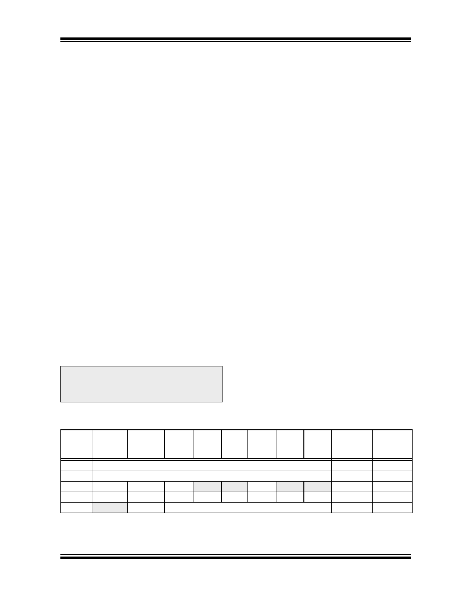
TABLE 11-1:
REGISTERS ASSOCIATED WITH TIMER0
Note:
Writing to TMR0 when the prescaler is
assigned to Timer0 will clear the prescaler
count, but will not change the prescaler
assignment.
Name
Bit 7
Bit 6
Bit 5
Bit 4
Bit 3
Bit 2
Bit 1
Bit 0
Value on
POR, BOR
Value on all
other
Resets
TMR0L
Timer0 Low Byte Register
xxxx xxxx uuuu uuuu
TMR0H
Timer0 High Byte Register
0000 0000 uuuu uuuu
INTCON
GIE/GIEH PEIE/GIEL TMR0IE INT0IE
RBIE
TMR0IF INT0IF
RBIF
0000 000x 0000 000u
T0CON
TMR0ON
T08BIT
T0CS
T0SE
PSA
T0PS2
T0PS1
T0PS0 1111 1111 1111 1111
TRISA
—
TRISA6(1) PORTA Data Direction Register
-111 1111 -111 1111
Legend:
x
= unknown, u = unchanged, — = unimplemented locations, read as ‘0’. Shaded cells are not used by Timer0.
Note 1:
RA6 and associated bits are configured as port pins in RCIO and ECIO Oscillator modes only and read ‘0’
in all other oscillator modes.
相关PDF资料 |
PDF描述 |
|---|---|
| PIC18LF8622-I/PT | IC PIC MCU FLASH 32KX16 80TQFP |
| PIC18LF8627-I/PT | IC PIC MCU FLASH 48KX16 80TQFP |
| PIC18LF8680-I/PT | IC PIC MCU FLASH 32KX16 80TQFP |
| PIC18LF8720-I/PT | IC MCU FLASH 64KX16 LV 80-TQFP |
| PIC18LF8722-I/PT | IC PIC MCU FLASH 64KX16 80TQFP |
相关代理商/技术参数 |
参数描述 |
|---|---|
| PIC18LF8621T-I/PT | 功能描述:8位微控制器 -MCU 64KB 3840 RAM 68I/O RoHS:否 制造商:Silicon Labs 核心:8051 处理器系列:C8051F39x 数据总线宽度:8 bit 最大时钟频率:50 MHz 程序存储器大小:16 KB 数据 RAM 大小:1 KB 片上 ADC:Yes 工作电源电压:1.8 V to 3.6 V 工作温度范围:- 40 C to + 105 C 封装 / 箱体:QFN-20 安装风格:SMD/SMT |
| PIC18LF8622-I/PT | 功能描述:8位微控制器 -MCU 64 KB FL 4K RAM 70 I/O RoHS:否 制造商:Silicon Labs 核心:8051 处理器系列:C8051F39x 数据总线宽度:8 bit 最大时钟频率:50 MHz 程序存储器大小:16 KB 数据 RAM 大小:1 KB 片上 ADC:Yes 工作电源电压:1.8 V to 3.6 V 工作温度范围:- 40 C to + 105 C 封装 / 箱体:QFN-20 安装风格:SMD/SMT |
| PIC18LF8622T-I/PT | 功能描述:8位微控制器 -MCU 64 KB FL 4K RAM 70 I/O RoHS:否 制造商:Silicon Labs 核心:8051 处理器系列:C8051F39x 数据总线宽度:8 bit 最大时钟频率:50 MHz 程序存储器大小:16 KB 数据 RAM 大小:1 KB 片上 ADC:Yes 工作电源电压:1.8 V to 3.6 V 工作温度范围:- 40 C to + 105 C 封装 / 箱体:QFN-20 安装风格:SMD/SMT |
| PIC18LF8627-I/PT | 功能描述:8位微控制器 -MCU 96 KB FL 4K RAM 70 I/O RoHS:否 制造商:Silicon Labs 核心:8051 处理器系列:C8051F39x 数据总线宽度:8 bit 最大时钟频率:50 MHz 程序存储器大小:16 KB 数据 RAM 大小:1 KB 片上 ADC:Yes 工作电源电压:1.8 V to 3.6 V 工作温度范围:- 40 C to + 105 C 封装 / 箱体:QFN-20 安装风格:SMD/SMT |
| PIC18LF8627T-I/PT | 功能描述:8位微控制器 -MCU 96 KB FL 4K RAM 70 I/O RoHS:否 制造商:Silicon Labs 核心:8051 处理器系列:C8051F39x 数据总线宽度:8 bit 最大时钟频率:50 MHz 程序存储器大小:16 KB 数据 RAM 大小:1 KB 片上 ADC:Yes 工作电源电压:1.8 V to 3.6 V 工作温度范围:- 40 C to + 105 C 封装 / 箱体:QFN-20 安装风格:SMD/SMT |
发布紧急采购,3分钟左右您将得到回复。