- 您现在的位置:买卖IC网 > PDF目录11749 > PIC24FJ96GA006-I/MR (Microchip Technology)MCU 96KB FLASH 8KB RAM 64-QFN PDF资料下载
参数资料
| 型号: | PIC24FJ96GA006-I/MR |
| 厂商: | Microchip Technology |
| 文件页数: | 10/258页 |
| 文件大小: | 0K |
| 描述: | MCU 96KB FLASH 8KB RAM 64-QFN |
| 特色产品: | PIC24FJ/33FJ MCUs & dsPIC? DSCs |
| 标准包装: | 40 |
| 系列: | PIC® 24F |
| 核心处理器: | PIC |
| 芯体尺寸: | 16-位 |
| 速度: | 16MHz |
| 连通性: | I²C,PMP,SPI,UART/USART |
| 外围设备: | 欠压检测/复位,POR,PWM,WDT |
| 输入/输出数: | 53 |
| 程序存储器容量: | 96KB(32K x 24) |
| 程序存储器类型: | 闪存 |
| RAM 容量: | 8K x 8 |
| 电压 - 电源 (Vcc/Vdd): | 2 V ~ 3.6 V |
| 数据转换器: | A/D 16x10b |
| 振荡器型: | 内部 |
| 工作温度: | -40°C ~ 85°C |
| 封装/外壳: | 64-QFN |
| 包装: | 管件 |
第1页第2页第3页第4页第5页第6页第7页第8页第9页当前第10页第11页第12页第13页第14页第15页第16页第17页第18页第19页第20页第21页第22页第23页第24页第25页第26页第27页第28页第29页第30页第31页第32页第33页第34页第35页第36页第37页第38页第39页第40页第41页第42页第43页第44页第45页第46页第47页第48页第49页第50页第51页第52页第53页第54页第55页第56页第57页第58页第59页第60页第61页第62页第63页第64页第65页第66页第67页第68页第69页第70页第71页第72页第73页第74页第75页第76页第77页第78页第79页第80页第81页第82页第83页第84页第85页第86页第87页第88页第89页第90页第91页第92页第93页第94页第95页第96页第97页第98页第99页第100页第101页第102页第103页第104页第105页第106页第107页第108页第109页第110页第111页第112页第113页第114页第115页第116页第117页第118页第119页第120页第121页第122页第123页第124页第125页第126页第127页第128页第129页第130页第131页第132页第133页第134页第135页第136页第137页第138页第139页第140页第141页第142页第143页第144页第145页第146页第147页第148页第149页第150页第151页第152页第153页第154页第155页第156页第157页第158页第159页第160页第161页第162页第163页第164页第165页第166页第167页第168页第169页第170页第171页第172页第173页第174页第175页第176页第177页第178页第179页第180页第181页第182页第183页第184页第185页第186页第187页第188页第189页第190页第191页第192页第193页第194页第195页第196页第197页第198页第199页第200页第201页第202页第203页第204页第205页第206页第207页第208页第209页第210页第211页第212页第213页第214页第215页第216页第217页第218页第219页第220页第221页第222页第223页第224页第225页第226页第227页第228页第229页第230页第231页第232页第233页第234页第235页第236页第237页第238页第239页第240页第241页第242页第243页第244页第245页第246页第247页第248页第249页第250页第251页第252页第253页第254页第255页第256页第257页第258页
2005-2012 Microchip Technology Inc.
DS39747F-page 107
PIC24FJ128GA010 FAMILY
10.0
I/O PORTS
All of the device pins (except VDD, VSS, MCLR and
OSC1/CLKI) are shared between the peripherals and
the parallel I/O ports. All I/O input ports feature Schmitt
Trigger inputs for improved noise immunity.
10.1
Parallel I/O (PIO) Ports
A parallel I/O port that shares a pin with a peripheral is,
in general, subservient to the peripheral. The periph-
eral’s output buffer data and control signals are
provided to a pair of multiplexers. The multiplexers
select whether the peripheral or the associated port
has ownership of the output data and control signals of
the I/O pin. The logic also prevents “loop through”, in
which a port’s digital output can drive the input of a
peripheral that shares the same pin. Figure 10-1 shows
how ports are shared with other peripherals and the
associated I/O pin to which they are connected.
When a peripheral is enabled and the peripheral is
actively driving an associated pin, the use of the pin as
a general purpose output pin is disabled. The I/O pin
may be read, but the output driver for the parallel port
bit will be disabled. If a peripheral is enabled, but the
peripheral is not actively driving a pin, that pin may be
driven by a port.
All port pins have three registers directly associated
with their operation as digital I/O. The Data Direction
register (TRISx) determines whether the pin is an input
or an output. If the data direction bit is a ‘1’, then the pin
is an input. All port pins are defined as inputs after a
Reset. Reads from the latch (LATx), read the latch.
Writes to the latch, write the latch. Reads from the port
(PORTx), read the port pins, while writes to the port
pins, write the latch.
Any bit and its associated data and control registers
that are not valid for a particular device will be
disabled. That means the corresponding LATx and
TRISx registers, and the port pin will read as zeros.
When a pin is shared with another peripheral or func-
tion that is defined as an input only, it is nevertheless,
regarded as a dedicated port because there is no
other competing source of outputs. An example is the
INT4 pin.
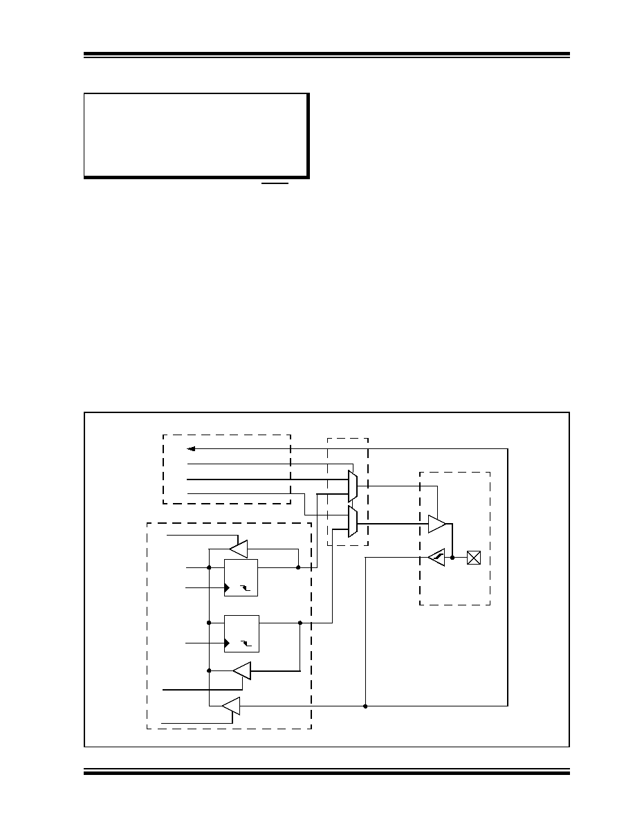
FIGURE 10-1:
BLOCK DIAGRAM OF A TYPICAL SHARED PORT STRUCTURE
Note:
This data sheet summarizes the features
of this group of PIC24F devices. It is not
intended to be a comprehensive refer-
ence source. Refer to Section 12. “I/O
Ports with Peripheral Pin Select (PPS)”
(DS39711)
in
the
“PIC24F
Family
Reference Manual”
for more information.
Q
D
CK
WR LAT +
TRIS Latch
I/O Pin
WR PORT
Data Bus
Q
D
CK
Data Latch
Read PORT
Read TRIS
1
0
1
0
WR TRIS
Peripheral Output Data
Output Enable
Peripheral Input Data
I/O
Peripheral Module
Peripheral Output Enable
PIO Module
Output Multiplexers
Output Data
Input Data
Peripheral Module Enable
Read LAT
相关PDF资料 |
PDF描述 |
|---|---|
| D38999/20FD97SB | CONN RCPT 12POS WALL MNT W/SCKT |
| MS3101F28-15S | CONN RCPT 35POS FREE HNG W/SCKT |
| VE-B0T-IX-F2 | CONVERTER MOD DC/DC 6.5V 75W |
| VE-B0M-IX-F4 | CONVERTER MOD DC/DC 10V 75W |
| PIC18LF27J13-I/SP | IC PIC MCU 128KB FLASH 28SPDIP |
相关代理商/技术参数 |
参数描述 |
|---|---|
| PIC24FJ96GA006T-I/PT | 功能描述:16位微控制器 - MCU 96KB 53 I/O RoHS:否 制造商:Texas Instruments 核心:RISC 处理器系列:MSP430FR572x 数据总线宽度:16 bit 最大时钟频率:24 MHz 程序存储器大小:8 KB 数据 RAM 大小:1 KB 片上 ADC:Yes 工作电源电压:2 V to 3.6 V 工作温度范围:- 40 C to + 85 C 封装 / 箱体:VQFN-40 安装风格:SMD/SMT |
| PIC24FJ96GA008 | 制造商:MICROCHIP 制造商全称:Microchip Technology 功能描述:PIC24FJ128GA010 Family Rev. A4 Silicon Errata |
| PIC24FJ96GA008-I/PT | 功能描述:16位微控制器 - MCU 96KB 69 I/O RoHS:否 制造商:Texas Instruments 核心:RISC 处理器系列:MSP430FR572x 数据总线宽度:16 bit 最大时钟频率:24 MHz 程序存储器大小:8 KB 数据 RAM 大小:1 KB 片上 ADC:Yes 工作电源电压:2 V to 3.6 V 工作温度范围:- 40 C to + 85 C 封装 / 箱体:VQFN-40 安装风格:SMD/SMT |
| PIC24FJ96GA008T-I/PT | 功能描述:16位微控制器 - MCU 96KB 69 I/O RoHS:否 制造商:Texas Instruments 核心:RISC 处理器系列:MSP430FR572x 数据总线宽度:16 bit 最大时钟频率:24 MHz 程序存储器大小:8 KB 数据 RAM 大小:1 KB 片上 ADC:Yes 工作电源电压:2 V to 3.6 V 工作温度范围:- 40 C to + 85 C 封装 / 箱体:VQFN-40 安装风格:SMD/SMT |
| PIC24FJ96GA010 | 制造商:MICROCHIP 制造商全称:Microchip Technology 功能描述:PIC24FJ128GA010 Family Rev. A4 Silicon Errata |
发布紧急采购,3分钟左右您将得到回复。