- 您现在的位置:买卖IC网 > PDF目录11749 > PIC24HJ128GP202-E/SP (Microchip Technology)IC PIC MCU FLASH 128K 28-DIP PDF资料下载
参数资料
| 型号: | PIC24HJ128GP202-E/SP |
| 厂商: | Microchip Technology |
| 文件页数: | 27/84页 |
| 文件大小: | 0K |
| 描述: | IC PIC MCU FLASH 128K 28-DIP |
| 标准包装: | 15 |
| 系列: | PIC® 24H |
| 核心处理器: | PIC |
| 芯体尺寸: | 16-位 |
| 速度: | 40 MIP |
| 连通性: | I²C,IrDA,LIN,PMP,SPI,UART/USART |
| 外围设备: | 欠压检测/复位,DMA,POR,PWM,WDT |
| 输入/输出数: | 21 |
| 程序存储器容量: | 128KB(43K x 24) |
| 程序存储器类型: | 闪存 |
| RAM 容量: | 8K x 8 |
| 电压 - 电源 (Vcc/Vdd): | 3 V ~ 3.6 V |
| 数据转换器: | A/D 10x10b/12b |
| 振荡器型: | 内部 |
| 工作温度: | -40°C ~ 125°C |
| 封装/外壳: | 28-DIP(0.300",7.62mm) |
| 包装: | 管件 |
| 配用: | AC164337-ND - MODULE SOCKET FOR PM3 40DIP |
第1页第2页第3页第4页第5页第6页第7页第8页第9页第10页第11页第12页第13页第14页第15页第16页第17页第18页第19页第20页第21页第22页第23页第24页第25页第26页当前第27页第28页第29页第30页第31页第32页第33页第34页第35页第36页第37页第38页第39页第40页第41页第42页第43页第44页第45页第46页第47页第48页第49页第50页第51页第52页第53页第54页第55页第56页第57页第58页第59页第60页第61页第62页第63页第64页第65页第66页第67页第68页第69页第70页第71页第72页第73页第74页第75页第76页第77页第78页第79页第80页第81页第82页第83页第84页
2010 Microchip Technology Inc.
DS70152H-page 33
dsPIC33F/PIC24H PROGRAMMING SPECIFICATION
5.2
Entering ICSP Mode
As illustrated in Figure 5-5, entering ICSP Program/
Verify mode requires three steps:
1.
MCLR is briefly driven high then low (P21)(1).
2.
A 32-bit key sequence is clocked into PGDx.
3.
MCLR is then driven high within a specified
period of time and held.
The programming voltage applied to MCLR is VIH,
which is essentially VDD in the case of dsPIC33F/
PIC24H devices. There is no minimum time require-
ment for holding at VIH. After VIH is removed, an interval
of at least P18 must elapse before presenting the key
sequence on PGDx.
The key sequence is a specific 32-bit pattern,
‘0100 1101 0100 0011 0100 1000 0101 0001’
(more
easily
remembered
as
0x4D434851
in
hexadecimal). The device will enter Program/Verify
mode only if the sequence is valid. The Most Significant
bit of the most significant nibble must be shifted in first.
Once the key sequence is complete, VIH must be
applied to MCLR and held at that level for as long as
Program/Verify mode is to be maintained. An interval of
at least time P19 and P7 must elapse before presenting
data on PGDx. Signals appearing on PGDx before P7
has elapsed will not be interpreted as valid.
On successful entry, the program memory can be
accessed and programmed in serial fashion. While in
ICSP mode, all unused I/Os are placed in the
high-impedance state.
5.3
ICSP Operation
After entering into ICSP mode, the CPU is Idle.
Execution of the CPU is governed by an internal state
machine. A 4-bit control code is clocked in using PGCx
and PGDx and this control code is used to command the
CPU (see Table 5-1).
The SIX control code is used to send instructions to the
CPU for execution and the REGOUT control code is
used to read data out of the device via the VISI register.
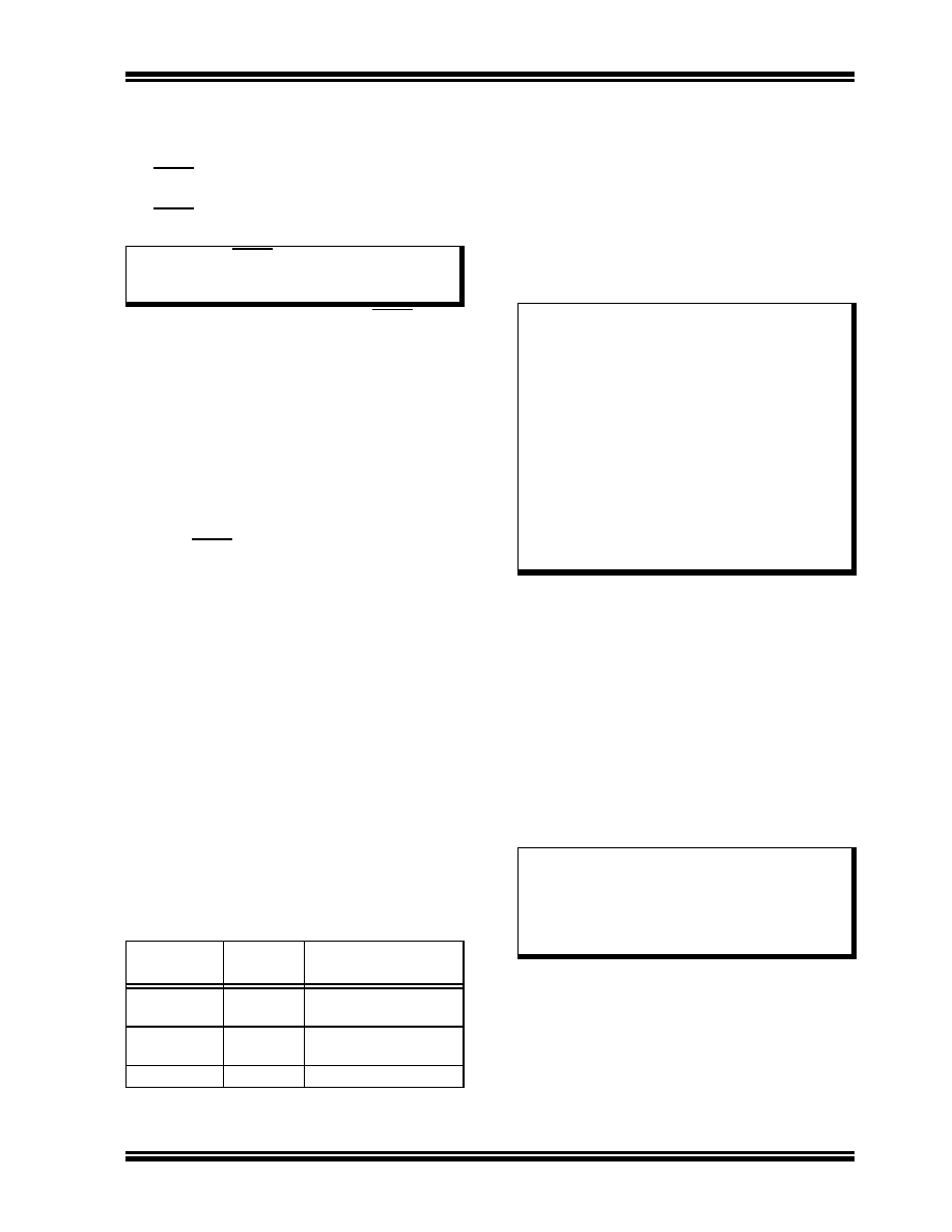
TABLE 5-1:
CPU CONTROL CODES IN
ICSP MODE
5.3.1
SIX SERIAL INSTRUCTION
EXECUTION
The SIX control code allows execution of dsPIC33F/
PIC24H Programming Specification assembly instruc-
tions. When the SIX code is received, the CPU is sus-
pended for 24 clock cycles, as the instruction is then
clocked into the internal buffer. Once the instruction is
shifted in, the state machine allows it to be executed over
the next four clock cycles. While the received instruction
is executed, the state machine simultaneously shifts in
the next 4-bit command (see Figure 5-3).
5.3.2
REGOUT SERIAL INSTRUCTION
EXECUTION
The REGOUT control code allows for data to be
extracted from the device in ICSP mode. It is used to
clock the contents of the VISI register out of the device
over the PGDx pin. After the REGOUT control code is
received, the CPU is held Idle for eight cycles. After these
eight cycles, an additional 16 cycles are required to clock
the data out (see Figure 5-4).
The REGOUT code is unique because the PGDx pin is
an input when the control code is transmitted to the
device. However, after the control code is processed,
the PGDx pin becomes an output as the VISI register is
shifted out.
Note 1: The MCLR capacitor value can vary the
high time required for entering ICSP
mode.
4-Bit
Control Code
Mnemonic
Description
0000b
SIX
Shift in 24-bit instruction
and execute.
0001b
REGOUT
Shift out the VISI
register.
0010b-1111b
N/A
Reserved.
Note 1: Coming out of the ICSP entry sequence,
the first 4-bit control code is always
forced to SIX and a forced NOP instruction
is executed by the CPU. Five additional
PGCx clocks are needed on start-up,
thereby resulting in a 9-bit SIX command
instead of the normal 4-bit SIX command.
After the forced SIX is clocked in, ICSP
operation resumes as normal (the next
24 clock cycles load the first instruction
word to the CPU). See Figure 5-2 for
details.
2: TBLRDH, TBLRDL, TBLWTH and TBLWTL
instructions must be followed by a NOP
instruction.
Note:
The device will latch input PGDx data on
the rising edge of PGCx and will output
data on the PGDx line on the rising edge
of PGCx. For all data transmissions, the
Least Significant bit (LSb) is transmitted
first.
相关PDF资料 |
PDF描述 |
|---|---|
| MS27468E17F99S | CONN RCPT 23POS JAM NUT W/SCKT |
| MCZ33781EK | IC MASTER DSI 2.02 DIFF 32-SOIC |
| MS27484E14B18PB | CONN PLUG 18POS STRAIGHT W/PINS |
| PIC18LF4221-I/ML | IC PIC MCU FLASH 2KX16 44QFN |
| VE-B4D-IX-F3 | CONVERTER MOD DC/DC 85V 75W |
相关代理商/技术参数 |
参数描述 |
|---|---|
| PIC24HJ128GP202-I/MM | 功能描述:16位微控制器 - MCU 16B MCU 28LD128KB DMA 40MIPS RoHS:否 制造商:Texas Instruments 核心:RISC 处理器系列:MSP430FR572x 数据总线宽度:16 bit 最大时钟频率:24 MHz 程序存储器大小:8 KB 数据 RAM 大小:1 KB 片上 ADC:Yes 工作电源电压:2 V to 3.6 V 工作温度范围:- 40 C to + 85 C 封装 / 箱体:VQFN-40 安装风格:SMD/SMT |
| PIC24HJ128GP202-I/SO | 功能描述:16位微控制器 - MCU 16B MCU 28LD128KB DMA 40MIPS RoHS:否 制造商:Texas Instruments 核心:RISC 处理器系列:MSP430FR572x 数据总线宽度:16 bit 最大时钟频率:24 MHz 程序存储器大小:8 KB 数据 RAM 大小:1 KB 片上 ADC:Yes 工作电源电压:2 V to 3.6 V 工作温度范围:- 40 C to + 85 C 封装 / 箱体:VQFN-40 安装风格:SMD/SMT |
| PIC24HJ128GP202-I/SP | 功能描述:16位微控制器 - MCU 16B MCU 28LD128KB DMA 40MIPS RoHS:否 制造商:Texas Instruments 核心:RISC 处理器系列:MSP430FR572x 数据总线宽度:16 bit 最大时钟频率:24 MHz 程序存储器大小:8 KB 数据 RAM 大小:1 KB 片上 ADC:Yes 工作电源电压:2 V to 3.6 V 工作温度范围:- 40 C to + 85 C 封装 / 箱体:VQFN-40 安装风格:SMD/SMT |
| PIC24HJ128GP202T-I/MM | 功能描述:16位微控制器 - MCU 16B MCU 28LD128KB DMA 40MIPS RoHS:否 制造商:Texas Instruments 核心:RISC 处理器系列:MSP430FR572x 数据总线宽度:16 bit 最大时钟频率:24 MHz 程序存储器大小:8 KB 数据 RAM 大小:1 KB 片上 ADC:Yes 工作电源电压:2 V to 3.6 V 工作温度范围:- 40 C to + 85 C 封装 / 箱体:VQFN-40 安装风格:SMD/SMT |
| PIC24HJ128GP202T-I/SO | 功能描述:16位微控制器 - MCU 16B MCU 28LD128KB DMA 40MIPS RoHS:否 制造商:Texas Instruments 核心:RISC 处理器系列:MSP430FR572x 数据总线宽度:16 bit 最大时钟频率:24 MHz 程序存储器大小:8 KB 数据 RAM 大小:1 KB 片上 ADC:Yes 工作电源电压:2 V to 3.6 V 工作温度范围:- 40 C to + 85 C 封装 / 箱体:VQFN-40 安装风格:SMD/SMT |
发布紧急采购,3分钟左右您将得到回复。