- 您现在的位置:买卖IC网 > PDF目录11475 > PIC24HJ32GP202T-I/SS (Microchip Technology)MCU PIC 16BIT 32K FLASH 28SSOP PDF资料下载
参数资料
| 型号: | PIC24HJ32GP202T-I/SS |
| 厂商: | Microchip Technology |
| 文件页数: | 232/289页 |
| 文件大小: | 0K |
| 描述: | MCU PIC 16BIT 32K FLASH 28SSOP |
| 标准包装: | 2,100 |
| 系列: | PIC® 24H |
| 核心处理器: | PIC |
| 芯体尺寸: | 16-位 |
| 速度: | 40 MIP |
| 连通性: | I²C,IrDA,LIN,SPI,UART/USART |
| 外围设备: | 欠压检测/复位,POR,PWM,WDT |
| 输入/输出数: | 21 |
| 程序存储器容量: | 32KB(11K x 24) |
| 程序存储器类型: | 闪存 |
| RAM 容量: | 2K x 8 |
| 电压 - 电源 (Vcc/Vdd): | 3 V ~ 3.6 V |
| 数据转换器: | A/D 10x10b/12b |
| 振荡器型: | 内部 |
| 工作温度: | -40°C ~ 85°C |
| 封装/外壳: | 28-SSOP(0.209",5.30mm 宽) |
| 包装: | 带卷 (TR) |
第1页第2页第3页第4页第5页第6页第7页第8页第9页第10页第11页第12页第13页第14页第15页第16页第17页第18页第19页第20页第21页第22页第23页第24页第25页第26页第27页第28页第29页第30页第31页第32页第33页第34页第35页第36页第37页第38页第39页第40页第41页第42页第43页第44页第45页第46页第47页第48页第49页第50页第51页第52页第53页第54页第55页第56页第57页第58页第59页第60页第61页第62页第63页第64页第65页第66页第67页第68页第69页第70页第71页第72页第73页第74页第75页第76页第77页第78页第79页第80页第81页第82页第83页第84页第85页第86页第87页第88页第89页第90页第91页第92页第93页第94页第95页第96页第97页第98页第99页第100页第101页第102页第103页第104页第105页第106页第107页第108页第109页第110页第111页第112页第113页第114页第115页第116页第117页第118页第119页第120页第121页第122页第123页第124页第125页第126页第127页第128页第129页第130页第131页第132页第133页第134页第135页第136页第137页第138页第139页第140页第141页第142页第143页第144页第145页第146页第147页第148页第149页第150页第151页第152页第153页第154页第155页第156页第157页第158页第159页第160页第161页第162页第163页第164页第165页第166页第167页第168页第169页第170页第171页第172页第173页第174页第175页第176页第177页第178页第179页第180页第181页第182页第183页第184页第185页第186页第187页第188页第189页第190页第191页第192页第193页第194页第195页第196页第197页第198页第199页第200页第201页第202页第203页第204页第205页第206页第207页第208页第209页第210页第211页第212页第213页第214页第215页第216页第217页第218页第219页第220页第221页第222页第223页第224页第225页第226页第227页第228页第229页第230页第231页当前第232页第233页第234页第235页第236页第237页第238页第239页第240页第241页第242页第243页第244页第245页第246页第247页第248页第249页第250页第251页第252页第253页第254页第255页第256页第257页第258页第259页第260页第261页第262页第263页第264页第265页第266页第267页第268页第269页第270页第271页第272页第273页第274页第275页第276页第277页第278页第279页第280页第281页第282页第283页第284页第285页第286页第287页第288页第289页
2007-2011 Microchip Technology Inc.
DS70289J-page 47
PIC24HJ32GP202/204 AND PIC24HJ16GP304
5.0
FLASH PROGRAM MEMORY
The PIC24HJ32GP202/204 and PIC24HJ16GP304
devices contain internal Flash program memory to
store and execute application code. The memory is
readable, writable and erasable during normal
operation over the entire VDD range.
Flash memory can be programmed in two ways:
In-Circuit Serial Programming (ICSP)
programming capability
Run-Time Self-Programming (RTSP)
ICSP allows a device to be serially programmed while
in the end application circuit. This is done with two lines
for programming clock and programming data (one of
the alternate programming pin pairs: PGECx/PGEDx),
and three other lines for power (VDD), ground (VSS) and
Master Clear (MCLR). This allows customers to
manufacture boards with unprogrammed devices and
then program the microcontroller just before shipping
the product. This also allows the most recent firmware
or a custom firmware to be programmed.
RTSP is accomplished using TBLRD (table read) and
TBLWT
(table write) instructions. With RTSP, the user
application can write program memory data either in
‘blocks’ or ‘rows’ of 64 instructions (192 bytes) at a time
or a single program memory word, and erase program
memory in blocks or ‘pages’ of 512 instructions (1536
bytes) at a time.
5.1
Table Instructions and Flash
Programming
Regardless of the method used, all programming of
Flash memory is done with the table read and table
write instructions. These allow direct read and write
access to the program memory space from the data
memory while the device is in normal operating mode.
The 24-bit target address in the program memory is
formed using bits <7:0> of the TBLPAG register and the
Effective Address (EA) from a W register specified in
the table instruction, as shown in Figure 5-1.
The TBLRDL and the TBLWTL instructions are used to
read or write to the bits<15:0> of program memory.
TBLRDL
and TBLWTL can access program memory in
both Word and Byte modes.
The TBLRDH and TBLWTH instructions are used to read
or write to bits<23:16> of program memory. TBLRDH
and TBLWTH can also access program memory in Word
or Byte mode.
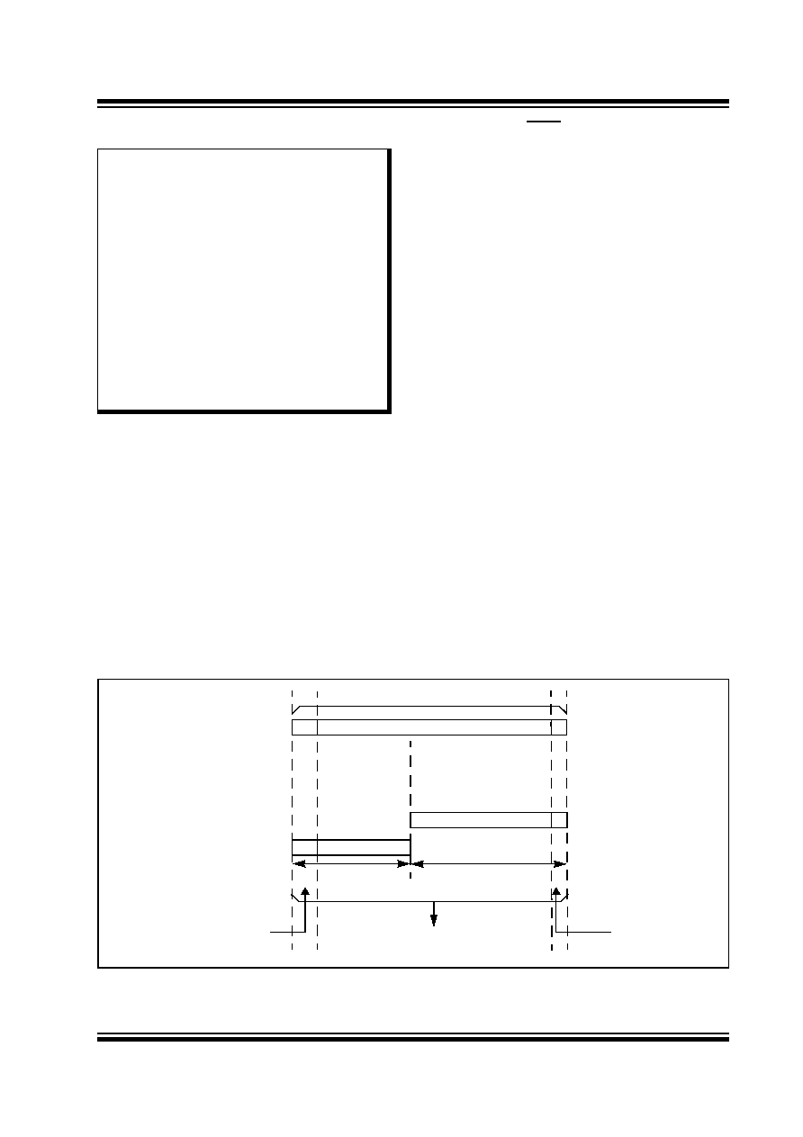
FIGURE 5-1:
ADDRESSING FOR TABLE REGISTERS
Note 1:
This data sheet summarizes the features
of
the
PIC24HJ32GP202/204
and
PIC24HJ16GP304 family of devices.
However, it is not intended to be a com-
prehensive reference source. To comple-
ment the information in this data sheet,
refer to “Section 4. Program Memory”
(DS70202) of the “dsPIC33F/PIC24H
Family Reference Manual”
, which is
available from the Microchip website
(www.microchip.com).
2:
Some registers and associated bits
described in this section may not be
available on all devices. Refer to
in
this data sheet for device-specific register
and bit information.
0
Program Counter
24 bits
Program Counter
TBLPAG Reg
8 bits
Working Reg EA
16 bits
Byte
24-bit EA
0
1/0
Select
Using
Table Instruction
Using
User/Configuration
Space Select
相关PDF资料 |
PDF描述 |
|---|---|
| PIC24FV16KA302-E/SP | IC MCU 16BIT 16KB FLASH 28SPDIP |
| VE-B2L-IW-S | CONVERTER MOD DC/DC 28V 100W |
| VE-B6M-CU-F1 | CONVERTER MOD DC/DC 10V 200W |
| VE-B6H-CU-F4 | CONVERTER MOD DC/DC 52V 200W |
| VE-B6H-CU-F3 | CONVERTER MOD DC/DC 52V 200W |
相关代理商/技术参数 |
参数描述 |
|---|---|
| PIC24HJ32GP203-E/ML | 制造商:MICROCHIP 制造商全称:Microchip Technology 功能描述:High-Performance, 16-bit Microcontrollers |
| PIC24HJ32GP203-E/MM | 制造商:MICROCHIP 制造商全称:Microchip Technology 功能描述:High-Performance, 16-bit Microcontrollers |
| PIC24HJ32GP203-E/PT | 制造商:MICROCHIP 制造商全称:Microchip Technology 功能描述:High-Performance, 16-bit Microcontrollers |
| PIC24HJ32GP203-E/SO | 制造商:MICROCHIP 制造商全称:Microchip Technology 功能描述:High-Performance, 16-bit Microcontrollers |
| PIC24HJ32GP203-E/SP | 制造商:MICROCHIP 制造商全称:Microchip Technology 功能描述:High-Performance, 16-bit Microcontrollers |
发布紧急采购,3分钟左右您将得到回复。