- 您现在的位置:买卖IC网 > PDF目录11544 > PIC32MX110F016BT-I/SO (Microchip Technology)32BIT MCU 16KB FLASH 28SOIC PDF资料下载
参数资料
| 型号: | PIC32MX110F016BT-I/SO |
| 厂商: | Microchip Technology |
| 文件页数: | 52/320页 |
| 文件大小: | 0K |
| 描述: | 32BIT MCU 16KB FLASH 28SOIC |
| 标准包装: | 1,600 |
| 系列: | PIC® 32MX |
| 核心处理器: | MIPS32? M4K? |
| 芯体尺寸: | 32-位 |
| 速度: | 40MHz |
| 连通性: | I²C,IrDA,LIN,PMP,SPI,UART/USART |
| 外围设备: | 欠压检测/复位,DMA,I²S,POR,PWM,WDT |
| 输入/输出数: | 21 |
| 程序存储器容量: | 16KB(16K x 8) |
| 程序存储器类型: | 闪存 |
| RAM 容量: | 4K x 8 |
| 电压 - 电源 (Vcc/Vdd): | 2.3 V ~ 3.6 V |
| 数据转换器: | A/D 10x10b |
| 振荡器型: | 内部 |
| 工作温度: | -40°C ~ 85°C |
| 封装/外壳: | 28-SOIC(0.295",7.50mm 宽) |
| 包装: | 带卷 (TR) |
第1页第2页第3页第4页第5页第6页第7页第8页第9页第10页第11页第12页第13页第14页第15页第16页第17页第18页第19页第20页第21页第22页第23页第24页第25页第26页第27页第28页第29页第30页第31页第32页第33页第34页第35页第36页第37页第38页第39页第40页第41页第42页第43页第44页第45页第46页第47页第48页第49页第50页第51页当前第52页第53页第54页第55页第56页第57页第58页第59页第60页第61页第62页第63页第64页第65页第66页第67页第68页第69页第70页第71页第72页第73页第74页第75页第76页第77页第78页第79页第80页第81页第82页第83页第84页第85页第86页第87页第88页第89页第90页第91页第92页第93页第94页第95页第96页第97页第98页第99页第100页第101页第102页第103页第104页第105页第106页第107页第108页第109页第110页第111页第112页第113页第114页第115页第116页第117页第118页第119页第120页第121页第122页第123页第124页第125页第126页第127页第128页第129页第130页第131页第132页第133页第134页第135页第136页第137页第138页第139页第140页第141页第142页第143页第144页第145页第146页第147页第148页第149页第150页第151页第152页第153页第154页第155页第156页第157页第158页第159页第160页第161页第162页第163页第164页第165页第166页第167页第168页第169页第170页第171页第172页第173页第174页第175页第176页第177页第178页第179页第180页第181页第182页第183页第184页第185页第186页第187页第188页第189页第190页第191页第192页第193页第194页第195页第196页第197页第198页第199页第200页第201页第202页第203页第204页第205页第206页第207页第208页第209页第210页第211页第212页第213页第214页第215页第216页第217页第218页第219页第220页第221页第222页第223页第224页第225页第226页第227页第228页第229页第230页第231页第232页第233页第234页第235页第236页第237页第238页第239页第240页第241页第242页第243页第244页第245页第246页第247页第248页第249页第250页第251页第252页第253页第254页第255页第256页第257页第258页第259页第260页第261页第262页第263页第264页第265页第266页第267页第268页第269页第270页第271页第272页第273页第274页第275页第276页第277页第278页第279页第280页第281页第282页第283页第284页第285页第286页第287页第288页第289页第290页第291页第292页第293页第294页第295页第296页第297页第298页第299页第300页第301页第302页第303页第304页第305页第306页第307页第308页第309页第310页第311页第312页第313页第314页第315页第316页第317页第318页第319页第320页
2011-2012 Microchip Technology Inc.
Preliminary
DS61168D-page 145
PIC32MX1XX/2XX
11.3
Peripheral Pin Select
A major challenge in general purpose devices is provid-
ing the largest possible set of peripheral features while
minimizing the conflict of features on I/O pins. The chal-
lenge is even greater on low pin-count devices. In an
application where more than one peripheral needs to
be assigned to a single pin, inconvenient workarounds
in application code or a complete redesign may be the
only option.
Peripheral pin select configuration provides an
alternative to these choices by enabling peripheral set
selection and their placement on a wide range of I/O
pins. By increasing the pinout options available on a
particular device, users can better tailor the device to
their entire application, rather than trimming the
application to fit the device.
The peripheral pin select configuration feature oper-
ates over a fixed subset of digital I/O pins. Users may
independently map the input and/or output of most dig-
ital peripherals to these I/O pins. Peripheral pin select
is performed in software and generally does not require
the device to be reprogrammed. Hardware safeguards
are included that prevent accidental or spurious
changes to the peripheral mapping once it has been
established.
11.3.1
AVAILABLE PINS
The number of available pins is dependent on the
particular device and its pin count. Pins that support the
peripheral pin select feature include the designation
“RPn” in their full pin designation, where “RP”
designates a remappable peripheral and “n” is the
remappable port number.
11.3.2
AVAILABLE PERIPHERALS
The peripherals managed by the peripheral pin select
are all digital-only peripherals. These include general
serial communications (UART and SPI), general pur-
pose timer clock inputs, timer-related peripherals (input
capture and output compare) and interrupt-on-change
inputs.
In comparison, some digital-only peripheral modules
are never included in the peripheral pin select feature.
This is because the peripheral’s function requires spe-
cial I/O circuitry on a specific port and cannot be easily
connected to multiple pins. These modules include I2C
among others. A similar requirement excludes all mod-
ules with analog inputs, such as the Analog-to-Digital
Converter (ADC).
A key difference between remappable and non-remap-
pable peripherals is that remappable peripherals are
not associated with a default I/O pin. The peripheral
must always be assigned to a specific I/O pin before it
can be used. In contrast, non-remappable peripherals
are always available on a default pin, assuming that the
peripheral is active and not conflicting with another
peripheral.
When a remappable peripheral is active on a given I/O
pin, it takes priority over all other digital I/O and digital
communication peripherals associated with the pin.
Priority is given regardless of the type of peripheral that
is mapped. Remappable peripherals never take priority
over any analog functions associated with the pin.
11.3.3
CONTROLLING PERIPHERAL PIN
SELECT
Peripheral pin select features are controlled through
two sets of SFRs: one to map peripheral inputs, and
one to map outputs. Because they are separately con-
trolled, a particular peripheral’s input and output (if the
peripheral has both) can be placed on any selectable
function pin without constraint.
The association of a peripheral to a peripheral-select-
able pin is handled in two different ways, depending on
whether an input or output is being mapped.
11.3.4
INPUT MAPPING
The inputs of the peripheral pin select options are
mapped on the basis of the peripheral. That is, a control
register associated with a peripheral dictates the pin it
will be mapped to. The [pin name]R registers, where [pin
name] refers to the peripheral pins listed in Table 11-1,
are used to configure peripheral input mapping (see
Register 11-1). Each register contains sets of 4 bit
fields. Programming these bit fields with an appropriate
value maps the RPn pin with the corresponding value to
that peripheral. For any given device, the valid range of
values for any bit field is shown in Table 11-1.
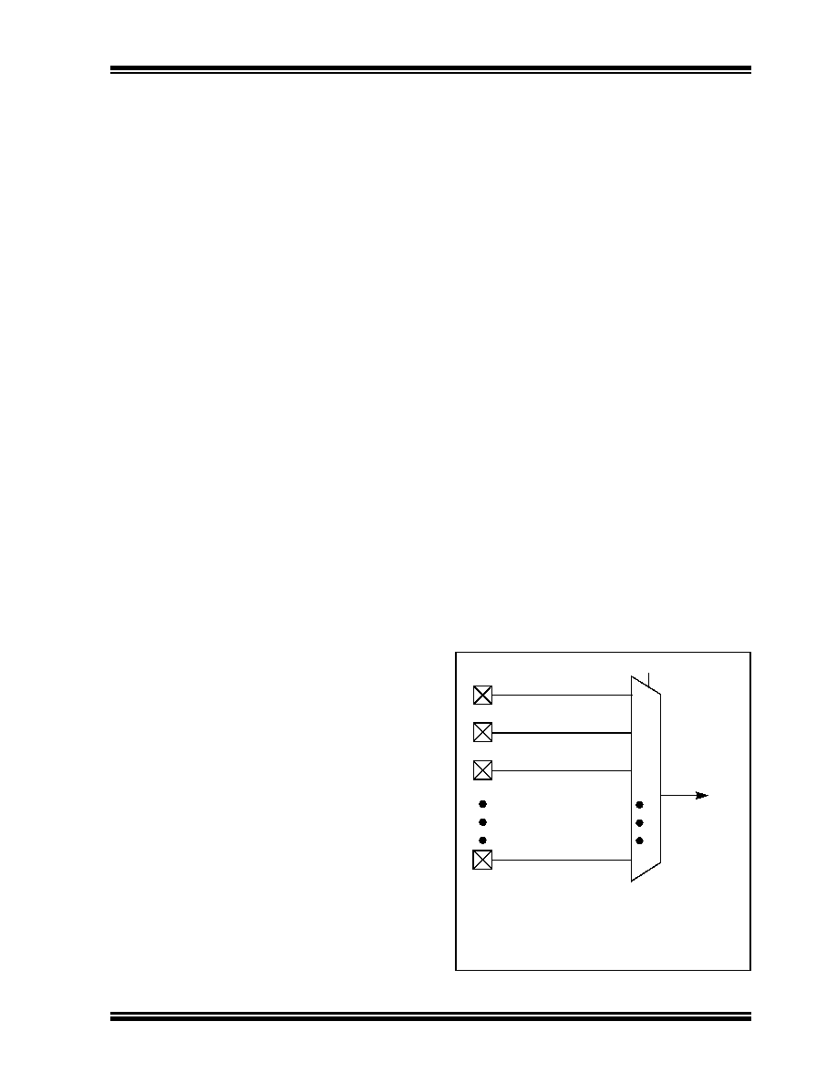
For example, Figure 11-2 illustrates the remappable
pin selection for the U1RX input.
FIGURE 11-2:
REMAPPABLE INPUT
EXAMPLE FOR U1RX
RPA2
RPB6
RPA4
0
1
2
U1RX input
U1RXR<3:0>
to peripheral
RPn
n
Note:
For input only, peripheral pin select functionality
does not have priority over TRISx settings.
Therefore, when configuring RPn pin for input,
the corresponding bit in the TRISx register must
also be configured for input (set to ‘1’).
相关PDF资料 |
PDF描述 |
|---|---|
| 226853-3 | CONN FEMALE CONTACT UHF TIN |
| DSPIC33FJ16MC101T-I/SO | IC DSC 16BIT 16KB 20SOIC |
| PIC24FJ16MC101T-I/SO | IC MCU 16BIT 16KB FLASH 20SOIC |
| PIC18LF43K22T-I/PT | IC MCU 8BIT 8KB FLASH 44TQFP |
| PIC18F43K22T-I/PT | IC MCU 8BIT 8KB FLASH 44TQFP |
相关代理商/技术参数 |
参数描述 |
|---|---|
| PIC32MX110F016BT-V/ML | 功能描述:32位微控制器 - MCU 32Bit MCU 16KB Fl 4KB RAM 40MHz 28Pin RoHS:否 制造商:Texas Instruments 核心:C28x 处理器系列:TMS320F28x 数据总线宽度:32 bit 最大时钟频率:90 MHz 程序存储器大小:64 KB 数据 RAM 大小:26 KB 片上 ADC:Yes 工作电源电压:2.97 V to 3.63 V 工作温度范围:- 40 C to + 105 C 封装 / 箱体:LQFP-80 安装风格:SMD/SMT |
| PIC32MX110F016BT-V/SO | 功能描述:32位微控制器 - MCU 32Bit MCU 16KB Fl 4KB RAM 40MHz 28Pin RoHS:否 制造商:Texas Instruments 核心:C28x 处理器系列:TMS320F28x 数据总线宽度:32 bit 最大时钟频率:90 MHz 程序存储器大小:64 KB 数据 RAM 大小:26 KB 片上 ADC:Yes 工作电源电压:2.97 V to 3.63 V 工作温度范围:- 40 C to + 105 C 封装 / 箱体:LQFP-80 安装风格:SMD/SMT |
| PIC32MX110F016BT-V/SS | 功能描述:32位微控制器 - MCU 32Bit MCU 16KB Fl 4KB RAM 40MHz 28Pin RoHS:否 制造商:Texas Instruments 核心:C28x 处理器系列:TMS320F28x 数据总线宽度:32 bit 最大时钟频率:90 MHz 程序存储器大小:64 KB 数据 RAM 大小:26 KB 片上 ADC:Yes 工作电源电压:2.97 V to 3.63 V 工作温度范围:- 40 C to + 105 C 封装 / 箱体:LQFP-80 安装风格:SMD/SMT |
| PIC32MX110F016B-V/ML | 功能描述:32位微控制器 - MCU PIC32 16KB FL 4KBR 40 MHz CTMU 4 DMA RoHS:否 制造商:Texas Instruments 核心:C28x 处理器系列:TMS320F28x 数据总线宽度:32 bit 最大时钟频率:90 MHz 程序存储器大小:64 KB 数据 RAM 大小:26 KB 片上 ADC:Yes 工作电源电压:2.97 V to 3.63 V 工作温度范围:- 40 C to + 105 C 封装 / 箱体:LQFP-80 安装风格:SMD/SMT |
| PIC32MX110F016B-V/SO | 功能描述:32位微控制器 - MCU PIC32 16KB FL 4KBR 40 MHz CTMU 4 DMA RoHS:否 制造商:Texas Instruments 核心:C28x 处理器系列:TMS320F28x 数据总线宽度:32 bit 最大时钟频率:90 MHz 程序存储器大小:64 KB 数据 RAM 大小:26 KB 片上 ADC:Yes 工作电源电压:2.97 V to 3.63 V 工作温度范围:- 40 C to + 105 C 封装 / 箱体:LQFP-80 安装风格:SMD/SMT |
发布紧急采购,3分钟左右您将得到回复。