- 您现在的位置:买卖IC网 > PDF目录98052 > PIIPM15P12D007 AC MOTOR CONTROLLER, 60 A PDF资料下载
参数资料
| 型号: | PIIPM15P12D007 |
| 元件分类: | 运动控制电子 |
| 英文描述: | AC MOTOR CONTROLLER, 60 A |
| 文件页数: | 3/25页 |
| 文件大小: | 1104K |
| 代理商: | PIIPM15P12D007 |
www.irf.com
11
PIIPM15P12D007
I27179 22 - Sep
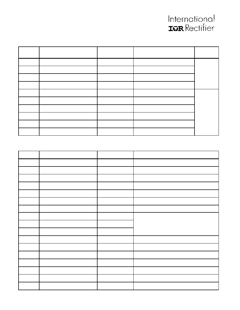
Other DSP pins mapping to the connector
Symbol
Signal Definition
DSP name ; pin N
Comments
Connector
Hall1
Hall effect sensor input 1
CAP4/QEP3/IOPE7 ; 60
Digital Input. See elec. characteristic of I/O pins
Hall2
Hall effect sensor input 2
CAP5/QEP4/IOPF0 ; 56
Digital Input. See elec. characteristic of I/O pins
Hall3 /
Excitation
Hall effect sensor input 3 / Resolver excitation
PWM7/IOPE1,
CAP6/IOPF1 ; 45, 48
Digital I/O, Output is type G3. See electrical
characteristics of I/O pins
Contactor
General purpose I/O
IOPB6 ; 11
Digital I/O, Output is type G3. See electrical
characteristics of I/O pins
RS485
CAN Tx
CAN transmit data
CANTX ; 50
Not isolated
CAN Rx
CAN receive data
CANRX ; 49
Not isolated
Homing/Direction
Homing signal/ Counter direction
TDIRB/IOPF4,
CAP3/IOPA5 ;2, 52
Avoid electrical conflicts beetwen these two pins
Start/Stop
Start/Stop signal
IOPF6 ; 92
Digital Input. See elec. Characteristic of I/O pins
Boot En~
Boot ROM enable signal
BOOT_EN~ ; 86
See also EDB electrical characteristics
Counter
Counter signal
TCLKINB ; 89
Digital Input. See elec. Characteristics of I/O pins
JTAG
These signals are internal only
Symbol
Signal Definition
DSP name ; pin N
Comments
PWM1
Out 1 high side IGBT gate drive signal
PWM1; 39
DSP Event Manager A output
PWM2
Out 1 low side IGBT gate drive signal
PWM2 ; 37
DSP Event Manager A output
PWM3
Out 2 high side IGBT gate drive signal
PWM3 ; 36
DSP Event Manager A output
PWM4
Out 2 low side IGBT gate drive signal
PWM4 ; 33
DSP Event Manager A output
PWM5
Out 3 high side IGBT gate drive signal
PWM5 ; 31
DSP Event Manager A output
PWM6
Out 3 low side IGBT gate drive signal
PWM6 ; 28
DSP Event Manager A output
Brake
Brake IGBT gate drive signal
T3PWM ; 7
DSP Event Manager B output
SpiTXout
SpiTx output
SPISIMO ; 21
SpiRXout
SpiRx input
SPISOMI ; 22
SpiCKout
SpiClk output
SPICLK ; 24
These signal are optically isolated.
See also EDB electrical characteristics
Ref3.3V
3.3V reference voltage
VREFHI, VCCA ; 82, 83
3.3V reference and supply voltage for ADC converter
5V supp.
Flash programming voltage pin
VCCP ; 40
Supplied by the embedded flyback regulator
Tx
SCI transmit data
SCITXD ; 17
Drives Tx+ and Tx- through the opto-isolator and the line driver
Rx
SCI receive data
SCIRXD ; 18
Driven by Rx+ and Rx- through the opto-isolator and the line driver
SCI_Tx_en
SCI transmitter enable
IOPA2 ; 16
Enable the SCI line driver through an opto-isolator
Latch-reset~
System general fault output reset signal
IOPD0 ; 15
LFAULT Reset signal, to be activated via software after a fault or
system boot, active low
FaultCLR
Gate driver fault output reset signal
IOPE3 ; 41
Gate driver reset, to be activated via software after a short-circuit or
system boot
相关PDF资料 |
PDF描述 |
|---|---|
| PIM200AZ | 1-OUTPUT 8 W DC-DC REG PWR SUPPLY MODULE |
| PIM200FZ | 1-OUTPUT 7.92 W DC-DC REG PWR SUPPLY MODULE |
| PIM300FZ | 2-OUTPUT 7.9 W DC-DC REG PWR SUPPLY MODULE |
| PIM300F6Z | 2-OUTPUT 7.9 W DC-DC REG PWR SUPPLY MODULE |
| PIP201-12M-3,518 | 200 A SWITCHING REGULATOR, PQCC68 |
相关代理商/技术参数 |
参数描述 |
|---|---|
| PIIPM25P12B008 | 制造商:未知厂家 制造商全称:未知厂家 功能描述:Programmable solated intelligent power module. a 25A. 1200V. three-phase inverter for 15kW industrial and servo motors with on-board programmable DSP. current sensing. isolation. gate drivers and power stage. |
| PIIPM25P12B008X | 功能描述:IC PWR MODULE PROG ISO 25A 1200V RoHS:否 类别:编程器,开发系统 >> 过时/停产零件编号 系列:- 标准包装:1 系列:* |
| PIIPM50E06A004 | 制造商:IRF 制造商全称:International Rectifier 功能描述:Programmable Isolated IPM |
| PIIPM50E06A004X | 制造商:IRF 制造商全称:International Rectifier 功能描述:Programmable Isolated IPM |
| PIIPM50E06B004 | 制造商:IRF 制造商全称:International Rectifier 功能描述:Programmable Isolated IPM |
发布紧急采购,3分钟左右您将得到回复。