- 您现在的位置:买卖IC网 > PDF目录96680 > PIN-1310-5I-50SMF-FCUPC FIBER OPTIC RECEIVER, 1260-1600nm, 10000Mbps, TO-46, FC/UPC CONNECTOR PDF资料下载
参数资料
| 型号: | PIN-1310-5I-50SMF-FCUPC |
| 元件分类: | 光接收 |
| 英文描述: | FIBER OPTIC RECEIVER, 1260-1600nm, 10000Mbps, TO-46, FC/UPC CONNECTOR |
| 文件页数: | 2/4页 |
| 文件大小: | 103K |
| 代理商: | PIN-1310-5I-50SMF-FCUPC |
PIN-1310-5I-XXX
5GHZ 1310NM PIN DIODE
NOTICE: Stresses greater than those listed under “Absolute
Maximum Ratings” may cause permanent damage to the
device. This is a stress rating only and functional operation
of the device at these or any other conditions above those
indicated in the operations section for extended periods of
time may affect reliability.
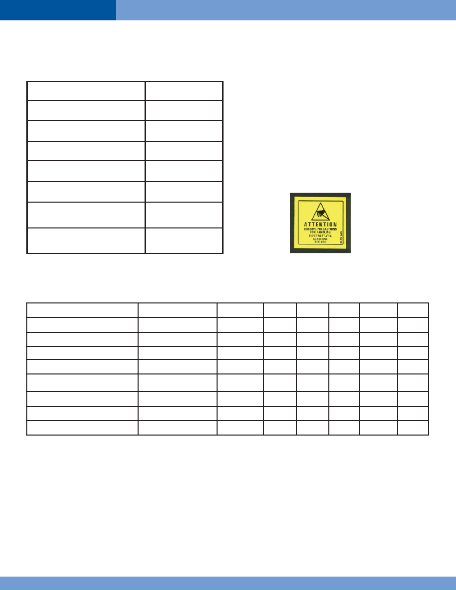
NOTICE: The inherent design of this component causes it
to be sensitive to electrostatic discharge (ESD). To prevent
ESD-induced damage and/or degradation to equipment,
take normal ESD precautions when handling this product.
ABSOLUTE MAXIMUM RATINGS
Parameter
Rating
Storage temperature
-40oC to +85oC
Case operating temperature
-40o to +85oC
Lead solder temperature
260oC, 10 seconds
PIN Reverse Voltage
10V
PIN Forward Current
2mA
Incident Optical Power
+6 dBm average,
+10 dBm peak
ESD exposure level (human body
model)
50V
ELECTRICAL-OPTICAL CHARACTERISTICS
TA = 25
oC unless otherwise stated
VCSEL Parameters
Test Condition
Symbol
Min.
Typ.
Max.
Units
Notes
Responsivity
λ1310nm, Vr=5v
R
0.80
0.85
mA/mW
1
Capacitance
F=100KHz
C
0.2
0.35
0.45
pF
2
Wavelength Response
λRESP
1260
1310
1600
nm
3
Dark Current
VR = 5V
IDARK
5
nA
PIN -3dB Bandwidth
Into 50
Ω, -5V bias
BW
6
7
GHz
4
Rise/Fall Time
P=0.1mW p-p
TR / TF
50
100
ps
5
Maximum Fiber Input Power
λ=1310nm
PMAX
3
mW
Optical Return Loss
ORL
23
dB
NOTES
1. Responsivity is for the entire pigtailed assembly, measured at 1310nm.
2. Capacitance is measured at 5V reverse bias. The PIN structure is fully depleted at less than 2V reverse bias.
3. Photodiode may respond to wavelengths outside this range, but is not guaranteed to do so.
4. Bandwidth is measured using small signal analysis.
5. The rise and fall times are measured using a laser source with transition times less than 30ps (20-80%), and an average power of 0.5mW.
相关PDF资料 |
PDF描述 |
|---|---|
| PJ11431CX | 1-OUTPUT TWO TERM VOLTAGE REFERENCE, 2.5 V, PDSO3 |
| PJ1301Y | SPECIALTY ANALOG CIRCUIT, PSSO3 |
| PJ130Y | SPECIALTY ANALOG CIRCUIT, PSSO3 |
| PJ1431CX | 1-OUTPUT TWO TERM VOLTAGE REFERENCE, 2.5 V, PDSO3 |
| PJ34063CD | 1.5 A SWITCHING REGULATOR, 100 kHz SWITCHING FREQ-MAX, PDIP8 |
相关代理商/技术参数 |
参数描述 |
|---|---|
| PIN1-3PIN2-3 | 制造商:PROTEC 制造商全称:Protek Devices 功能描述:600 WATT TVS ARRAY-ASYMMETRICAL DATA LINE PROTECTOR |
| PIN-1I | 制造商:SR COMPONENTS 功能描述: 制造商:SR Components Inc 功能描述: |
| PIN-1I-1000 | 制造商:SR Components Inc 功能描述: |
| PIN220D | 制造商:未知厂家 制造商全称:未知厂家 功能描述:Optoelectronic |
| PIN220DP | 制造商:未知厂家 制造商全称:未知厂家 功能描述:Optoelectronic |
发布紧急采购,3分钟左右您将得到回复。