- 您现在的位置:买卖IC网 > PDF目录96680 > PJ34063CS 1.5 A SWITCHING REGULATOR, 100 kHz SWITCHING FREQ-MAX, PDSO8 PDF资料下载
参数资料
| 型号: | PJ34063CS |
| 元件分类: | 稳压器 |
| 英文描述: | 1.5 A SWITCHING REGULATOR, 100 kHz SWITCHING FREQ-MAX, PDSO8 |
| 封装: | SOP-8 |
| 文件页数: | 2/8页 |
| 文件大小: | 351K |
| 代理商: | PJ34063CS |
PJ34063
DC-To-DC Converter Controller
2-8
2004/10 rev.B
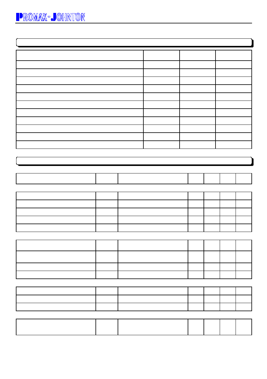
Characteristic
Symbol
Value
Unit
Power Supply Voltage
VCC
40
Vdc
Comparator Input Voltage Range
VIR
-0.3 ~ +40
Vdc
Switch Collector Voltage
VC(SW)
40
Vdc
Switch Emitter Voltage
VE(SW)
40
Vdc
Switch Collector to Emitter Voltage
VCE(SW)
40
Vdc
Driver Collector Voltage
VC(drive)
40
Vdc
Drive Collector Current (Note 1)
IC(drive)
100
mA
Switch Current
Isw
1.5
A
Operating Junction Temperature
TJ
0 to +125
℃
Operating Ambient Temperature Range
TA
-20 to +85
℃
Storage Temperature Range
Tstg
-25 to +150
℃
(VCC = 5.0V. Ta= Tlow to Thigh. unless otherwise specified)
Characteristic
Symbol
Test Condition
Min
Typ
Max
Unit
OSCILLATOR
Frequency
fosc
VPIN5=0V, CT=1.0nF , TA=25℃
24
33
42
KHz
Charging Current
Ichg
VCC=5 to 40V, TA=25℃
24
35
42
μ
A
Discharge Current
Idischg
VCC=5 to 40V, TA=25℃
140
220
260
μ
A
Discharge To Charge Current Ratio
Idischg/Ichg
Pin7 to VCC , TA=25℃
5.2
6.5
7.5
--
Current Limit Sense Voltage
VIPK(sense)
Ichg = Idischg, TA=25℃
250
300
350
mV
OUTPUT SWITCH(NOTE 2)
Saturation Voltage , Darlington
Connection
VCE(sat)
Isw=1.0A, Pins1,8 connected
--
1.0
1.3
V
Saturation Voltage , Darlington
Connection
VCE(sat)
Isw=1.0A, RPIN8=82Ω to Vcc,
Forced β≌20
--
0.45
0.7
V
DC Current Gain
hFE
Isw=1.0A, VCE = 5.0V, TA=25℃
50
75
--
Collector Off- State Current
IC(off)
VCE =40V
--
40
100
μ
A
COMPARATOR
Threshold Voltage
VTH
TA=25℃
1.23
1.25
1.27
V
Threshold Voltage Line Regulation
Regline
VCC = 3 to 40V
--
1.4
5.0
mV
Input Bias Current
IIB
VIN=0V
--
-20
-400
nA
TOTAL DEVICE
Supply Current
ICC
VCC=5 to 40V, CT=1.0nF,
Pin7=Vcc ,VPIN 5>Vth
Pin 2 =GND, remaining pins open
--
4.0
mA
Notes : 1.Maximum package power dissipation limits must be observed.
2.Low duty cycle pulse techniques are used during test to maintain junction temperature as close to ambient temperature
as possible.
ELECTRICAL CHARACTERISTICS
ABSOLUTE MAXIMUM RATINGS
相关PDF资料 |
PDF描述 |
|---|---|
| PJ3800CA | 0.05 A SWITCHING CONTROLLER, 1000 kHz SWITCHING FREQ-MAX, PDSO8 |
| PJ3800CS | 0.05 A SWITCHING CONTROLLER, 1000 kHz SWITCHING FREQ-MAX, PDSO8 |
| PKA2231CI | 3-OUTPUT 25 W DC-DC REG PWR SUPPLY MODULE |
| PKA2231P | 3-OUTPUT 25 W DC-DC REG PWR SUPPLY MODULE |
| PKA2232CI | 3-OUTPUT 25 W DC-DC REG PWR SUPPLY MODULE |
相关代理商/技术参数 |
参数描述 |
|---|---|
| PJ3800 | 制造商:未知厂家 制造商全称:未知厂家 功能描述:Low Voltage Switching Regulator Controller |
| PJ3800CA | 制造商:未知厂家 制造商全称:未知厂家 功能描述:Low Voltage Switching Regulator Controller |
| PJ3800CS | 制造商:未知厂家 制造商全称:未知厂家 功能描述:Low Voltage Switching Regulator Controller |
| PJ3842 | 制造商:未知厂家 制造商全称:未知厂家 功能描述:High Performance Current Mode Controller |
| PJ3842B | 制造商:未知厂家 制造商全称:未知厂家 功能描述:High Performance Current Mode Controller |
发布紧急采购,3分钟左右您将得到回复。