- 您现在的位置:买卖IC网 > PDF目录96680 > PJ3800CS 0.05 A SWITCHING CONTROLLER, 1000 kHz SWITCHING FREQ-MAX, PDSO8 PDF资料下载
参数资料
| 型号: | PJ3800CS |
| 元件分类: | 稳压器 |
| 英文描述: | 0.05 A SWITCHING CONTROLLER, 1000 kHz SWITCHING FREQ-MAX, PDSO8 |
| 封装: | SOP-8 |
| 文件页数: | 2/8页 |
| 文件大小: | 330K |
| 代理商: | PJ3800CS |
PJ3800
Low Voltage Switching Regulator Controller
2-8
2003/04.rev.A
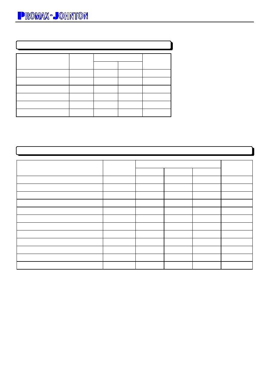
Rated Value
Parameter
Symbol
Min.
Max.
Unit
Power supply voltage
VCC
—
16
V
Output source current
IO+
—
-50
mA
Output sink current
IO-
—
50
mA
Allowable dissipation
PD
—
570*
mW
Operating temperature
Top
-30
+85
℃
Storage temperature
Tstg
-55
+125
℃
* : When mounted on a 10 cm square double-sided epoxy board
WARNING: Semiconductor devices can be permanently damaged by application of stress (voltage, current, temperature, etc.)
in excess of absolute maximum ratings. Do not exceed these ratings.
Values
Parameter
Symbol
Min.
Typ.
Max.
Unit
Power supply voltage
VCC
1.8
—
15
V
Error amplifier input voltage
VI
–
0.2
—
1
V
BR/CTL pin input voltage
VBR
–
0.2
—
VCC
V
Output source current
IO+
–
40
—
mA
Output sink current
IO–
—
40
mA
SCP pin capacitance
CPE
—
0.1
—
μ
F
Phase compensation capacitance
CP
—
0.1
—
μ
F
Output current setting resistance
RB
150
390
5000
Ω
Timing resistance
RT
1
3
10
kΩ
Timing capacitance
CT
100
270
10000
pF
Oscillation frequency
fOSC
10
500
1000
kHz
Operating temperature
TOP
–
30
+25
+85
℃
WARNING: Recommended operating conditions are normal operating ranges for the semiconductor device. All the device’s
electrical characteristics are warranted when operated within these ranges.
Always use semiconductor devices within the recommended operating conditions. Operation outside
these ranges may adversely affect reliability and could result in device failure.
No warranty is made with respect to uses, operating conditions, or combinations not represented on the data sheet.
Users considering application outside the listed conditions are advised to contact their Promax Johnton
representative beforehand.
ABSOLUTE MAXIMUM RATINGS
RECOMMENDED OPERATING CONDITIONS
相关PDF资料 |
PDF描述 |
|---|---|
| PKA2231CI | 3-OUTPUT 25 W DC-DC REG PWR SUPPLY MODULE |
| PKA2231P | 3-OUTPUT 25 W DC-DC REG PWR SUPPLY MODULE |
| PKA2232CI | 3-OUTPUT 25 W DC-DC REG PWR SUPPLY MODULE |
| PKA2212P | 1-OUTPUT 25 W DC-DC REG PWR SUPPLY MODULE |
| PKA2323CI | 2-OUTPUT 30 W DC-DC REG PWR SUPPLY MODULE |
相关代理商/技术参数 |
参数描述 |
|---|---|
| PJ3842 | 制造商:未知厂家 制造商全称:未知厂家 功能描述:High Performance Current Mode Controller |
| PJ3842B | 制造商:未知厂家 制造商全称:未知厂家 功能描述:High Performance Current Mode Controller |
| PJ3842BCD | 制造商:未知厂家 制造商全称:未知厂家 功能描述:High Performance Current Mode Controller |
| PJ3842BCS | 制造商:未知厂家 制造商全称:未知厂家 功能描述:High Performance Current Mode Controller |
| PJ3843 | 制造商:未知厂家 制造商全称:未知厂家 功能描述:High Performance Current Mode Controller |
发布紧急采购,3分钟左右您将得到回复。