- 您现在的位置:买卖IC网 > PDF目录98052 > PJ3842BCS 1 A SWITCHING CONTROLLER, 500 kHz SWITCHING FREQ-MAX, PDSO8 PDF资料下载
参数资料
| 型号: | PJ3842BCS |
| 元件分类: | 稳压器 |
| 英文描述: | 1 A SWITCHING CONTROLLER, 500 kHz SWITCHING FREQ-MAX, PDSO8 |
| 封装: | PLASTIC, SOP-8 |
| 文件页数: | 14/15页 |
| 文件大小: | 887K |
| 代理商: | PJ3842BCS |
PJ3842B / PJ3843B
High Performance Current Mode Controller
8-15
2002.ver.A
Output
These devices contain a single totem pole output stage
that was specifically designed for direct drive of power
MOSFET’s. It is capable of up to ±1.0A peak drive current
and has a typical rise and fall time of 50 ns with a 1.0nF load.
Additional internal circuitry has been added to keep the
Output in a sinking mode whenever an undervoltage lockout
is active.This characteristic eliminates the need for an
external pull-down resistor.
The SOP-8 surface mount package provides separate pins
for
Vc(output
supply)
and
Power
Ground.Proper
implementation will significantly reduce the level of
switching transient noise imposed on the control circuitry.
This becomes particularly useful when reducing the Ipk(max)
clamp level.The separate Vc supply input allows the designer
added fiexlbility in tailoring the drive voltage independent of
Vcc.A zener clamp is typically connected to this input when
driving power MOSFETs in systems where Vcc is greater
than 20V. Figure 25 shows proper power and control ground
connections in a current sensing power MOSFET application.
Reference
The 5.0V bandgap reference is trimmed to±2.0% on the
PJ3842B.Its promary purpose to supply charging current to
the oscillator timing capacitor.The reference has short circuit
protection and is capable of providing in excess of 20mA for
powering additional control system circuitry.
Design Considerations
Do not attempt to construct the converter on wirewrap or
plug-in prototype boards. High frequency circuit layout
techniques are imperative to prevent pulsewidth jitter.This is
usually caused by excessive noise pick-up imposed on the
Current Sense or Voltage Feedback inputs.Noise immunity
can be improved by lowering circuit impedances at these
points.The printed circuit layout should contain a ground
plane with lowcurrent signal and high-current switch and
output grounds returning separate paths back to the input
filter capacitor.Ceramic bypass capacitors(0.1μF) connected
directly to Vcc,Vc, and Vref may be required depending upon
circuit layout . This provides a low impedance path for
filtering the high frequency noised. All high current loops
should be kept as short as possible using heavy copper runs to
minimize radiated EMI. The Error Amp compensation
circuitry and the converter output voltage divider should be
located close to the IC and as far as possible from the power
switch and other noise generating components.
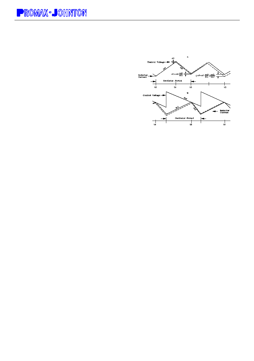
FIGURE 19-CONTINUOUS CURRENT WAVEFROMS
Current
mode
converters
can
exhibit
subharmonic
oscillations when operating at a duty cycle greater than 50%
with
continuous
inductor
current,This
instability
is
independent of the regulators closed loop characteristics and
is caused by the simultaneous operating conditions of fixed
frequency and peak current detecting. Figure 19A shows the
phenomenon graphically, At t0 , switch conduction begins ,
causing the inductor current to rise at a slope of m1. This
slope is a function of the input voltage divided by the
inductance. At t1, the Current Sense Input reaches the
threshold established by the control voltage. This causes the
switch to turn off and the current to decay at a slope of m2,
until the next oscillator cycle. This unstable condition can be
shown if a perturbation is added to the control voltage ,
resulting in a small Δl (dashed line). With a fixed oscillator
period, the current decay time is reduced, and the minimum
current at switch turn-on(t2) is increased by Δl+Δl m2/m1.
The minimum current at the next cycle (t3) decreases to (Δ
l+ Δ l m2/m1)(m2/m1). This perturbation is multiplied by
m2/m1 on each succeeding cycle , alternately increasing and
decreasing the inductor current at switch turn-on, Several
oscillator cycles may be required before the inductor current
reaches zero causing the process to commence again. If m2/m1
is greater than 1, the converter will be unstable . Figure 19B
shows that by adding an artificial ramp that is synchronized
with the PWM clock to the control voltage . the Δ l
perturbation will decrease to zero on succeeding cycles. This
compensating ramp (m3) must have a slope equal to or
slightly greater than m2/2 for stability . With m2/2 slope
compensation , the average inductor current follows the
control voltage yielding true current mode operation. The
compensating ramp can be derived from the oscillator and
added to either the Voltage Feedback or Current Sense inputs
(Figure 32).
相关PDF资料 |
PDF描述 |
|---|---|
| PJ3843BCD | 1 A SWITCHING CONTROLLER, 500 kHz SWITCHING FREQ-MAX, PDIP8 |
| PJ3845BCD | 1 A SWITCHING CONTROLLER, 500 kHz SWITCHING FREQ-MAX, PDIP8 |
| PJ3844BCD | 1 A SWITCHING CONTROLLER, 500 kHz SWITCHING FREQ-MAX, PDIP8 |
| PJ3845BCS | 1 A SWITCHING CONTROLLER, 500 kHz SWITCHING FREQ-MAX, PDSO8 |
| PJ431BCY | 1-OUTPUT TWO TERM VOLTAGE REFERENCE, 2.495 V, PSSO3 |
相关代理商/技术参数 |
参数描述 |
|---|---|
| PJ3843 | 制造商:未知厂家 制造商全称:未知厂家 功能描述:High Performance Current Mode Controller |
| PJ3843B | 制造商:未知厂家 制造商全称:未知厂家 功能描述:High Performance Current Mode Controller |
| PJ3843BCD | 制造商:未知厂家 制造商全称:未知厂家 功能描述:High Performance Current Mode Controller |
| PJ3843BCS | 制造商:未知厂家 制造商全称:未知厂家 功能描述:High Performance Current Mode Controller |
| PJ3844 | 制造商:未知厂家 制造商全称:未知厂家 功能描述:High Performance Current Mode Controller |
发布紧急采购,3分钟左右您将得到回复。