- 您现在的位置:买卖IC网 > PDF目录370005 > PLF8577C (NXP Semiconductors N.V.) LCD direct/duplex driver with I2C-bus interface PDF资料下载
参数资料
| 型号: | PLF8577C |
| 厂商: | NXP Semiconductors N.V. |
| 英文描述: | LCD direct/duplex driver with I2C-bus interface |
| 中文描述: | 液晶直接/双工司机带I2C总线接口 |
| 文件页数: | 8/28页 |
| 文件大小: | 195K |
| 代理商: | PLF8577C |
第1页第2页第3页第4页第5页第6页第7页当前第8页第9页第10页第11页第12页第13页第14页第15页第16页第17页第18页第19页第20页第21页第22页第23页第24页第25页第26页第27页第28页
1998 Jul 30
8
Philips Semiconductors
Product specification
LCD direct/duplex driver with
I
2
C-bus interface
PCF8577C
6.7
Power-on reset
At power-on reset the PCF8577C resets to a defined
starting condition as follows:
1.
Both backplane outputs are set to V
SS
in master mode;
to 3-state in cascade mode
2.
All segment outputs are set to V
SS
3.
The segment byte registers and control register are
cleared
4.
The I
2
C-bus interface is initialized.
6.8
Slave address
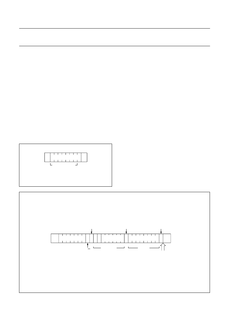
The PCF8577C slave address is shown in Fig.6.
Before any data is transmitted on the I
2
C-bus, the device
which should respond is addressed first. The addressing is
always done with the first byte transmitted after the start
procedure.
Fig.6 PCF8577C slave address.
0 1 1 1 0 1 0 0
S
A
SLAVE ADDRESS
MGA731
6.9
I
2
C-bus protocol
The PCF8577C I
2
C-bus protocol is shown in Fig.7.
The PCF8577C is a slave receiver and has a fixed slave
address (see Fig.6). All PCF8577Cs with the same slave
address acknowledge the slave address in parallel.
The second byte is always the control byte and is loaded
into the control register of each PCF8577C connected to
the I
2
C-bus. All addressed devices acknowledge the
control byte. Subsequent data bytes are loaded into the
segment registers of the selected device. Any number of
data bytes may be loaded in one transfer and in an
expanded system rollover of the SBV from 111 111 to
000 000 is allowed. If a stop (P) condition is given after the
control byte acknowledge the segment data will remain
unchanged. This allows the BANK bit to be toggled without
changing the segment register contents. During loading of
segment data only the selected PCF8577C gives an
acknowledge. Loading is terminated by generating a stop
(P) condition.
Fig.7 I
2
C-bus protocol.
S
A
SLAVE ADDRESS
A
A
SEGMENT DATA
P
acknowledge by
all PCF8577C
R/W
auto increment
segment byte vector
MGA732
0
M
B
SEGMENT
BYTE VECTOR
acknowledge by
all PCF8577C
acknowledge by
selected PCF8577C only
msb
lsb
n bytes
control byte
相关PDF资料 |
PDF描述 |
|---|---|
| PLL0930A | PHASE LOCKED LOOP |
| PLL1000A | PHASE LOCKED LOOP |
| PLL103-02 | DDR SDRAM Buffer for Desktop PCs with 4 DDR DIMMS |
| PLL103-02XC | DDR SDRAM Buffer for Desktop PCs with 4 DDR DIMMS |
| PLL103-02XI | DDR SDRAM Buffer for Desktop PCs with 4 DDR DIMMS |
相关代理商/技术参数 |
参数描述 |
|---|---|
| PLFF1000 | 功能描述:机架和机柜配件 5 PLEATED FILTERS XPFA80 RoHS:否 制造商:Bivar 产品:Rack Accessories 面板空间: 颜色:Black |
| PLFF2000 | 功能描述:机架和机柜配件 5 PLEATED FILTERS XPFA120 RoHS:否 制造商:Bivar 产品:Rack Accessories 面板空间: 颜色:Black |
| PLFF6000 | 功能描述:机架和机柜配件 5 PLEATED FILTERS XPFA254 RoHS:否 制造商:Bivar 产品:Rack Accessories 面板空间: 颜色:Black |
| PLFMTR4 | 制造商:Pyle 功能描述:SD / USB Flash Memory MP3 Player with FM Transmitter 制造商:PYLE 功能描述:USB / SD MP3 PLAYER W/REMOTE WITH FM TRANSMITTER |
| PLFN00183 | 制造商:Denon Electronics 功能描述:PR003 |
发布紧急采购,3分钟左右您将得到回复。