- 您现在的位置:买卖IC网 > PDF目录378051 > PM29F002B-70JC (PMC-Sierra, Inc.) 2 Megabit (256K X 8) 5.0 Volt-only CMOS Flash Memory PDF资料下载
参数资料
| 型号: | PM29F002B-70JC |
| 厂商: | PMC-Sierra, Inc. |
| 英文描述: | 2 Megabit (256K X 8) 5.0 Volt-only CMOS Flash Memory |
| 中文描述: | 2兆位(256K × 8)5.0伏,只有闪存的CMOS |
| 文件页数: | 5/21页 |
| 文件大小: | 148K |
| 代理商: | PM29F002B-70JC |
Programmable Microelectronics Corp.
Issue Date: March, 2001 Rev: 1.0
PMC
Pm29F002
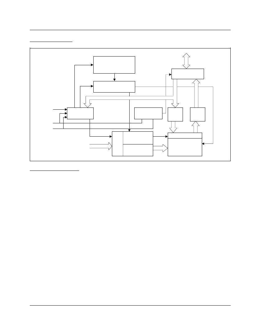
BLOCK DIAGRAM
DEVICE OPERATION
READ OPERATION
The access of Pm29F002 is similar as that of
EPROM. To obtain data at the outputs, three control
functions must be satisfied:
CE# is the chip enable and should be pulled low
( V
IL
).
OE# is the output enable and should be pulled
low ( V
IL
).
WE# is the write enable and should remains high
( V
IH
)
.
BOOT BLOCK LOCKOUT
The device has a software lockout feature to pre-
vent the data in the boot block from being erased or
reprogrammed. The boot block can be located at the
top or bottom of the address location. The block size is
16 Kbytes. Once the lockout feature is enable, the boot
block can not be erased or reprogrammed. Data in the
main memory block can still be updated through the
regular programming method. The boot block lockout
feature can be turned on by issuing a six-bus-cycle com-
mand sequence. Please refer to Table 4 and Chart 4.
BOOT BLOCK LOCKOUT DETECTION
The state of the Boot Block lockout can be de-
tected by software product identification entry. After
entry, selects Boot Block address with A0 =
“
0
”
and A1
=
“
1
”
and then read I/O0. A data of
“
0
”
means the lock-
out feature is disabled and the Boot Block can be erased
or programmed. A data of
“
1
”
means the lockout fea-
ture is enabled and the Boot Block is protected. Prod-
uct identification exit must be executed before the de-
vice returns to read mode.
PRODUCT IDENTIFICATION
The product identification mode can be used to identify
the device and the manufacturer by hardware or soft-
ware operation. The hardware operation mode is acti-
vated by applying a 12.0 Volt on A9 pin, typically used
by an external programmer to select the right program-
ming algorithm for the device. For detail, please see
Bus Operation Modes in Table 3. The software opera-
tion mode is activated by three-bus-cycle command.
Please see Software Command Definition in Table 4.
5
WE#
CE#
OE#
COMMAND
REGISTER
CE,OE LOGIC
A0-A17
ERASE/PROGRAM
VOLTAGE
GENERATOR
HIGH VOLTAGE
SWITCH
I/O0-I/O7
I/O BUFFERS
DATA
LATCH
SENSE
AMP
Y-GATING
MEMORY
ARRAY
A
L
Y-DECODER
X-DECODER
相关PDF资料 |
PDF描述 |
|---|---|
| PM29F002B-70PC | 2 Megabit (256K X 8) 5.0 Volt-only CMOS Flash Memory |
| PM29F002B-90JC | 2 Megabit (256K X 8) 5.0 Volt-only CMOS Flash Memory |
| PM29F002B-90PC | 2 Megabit (256K X 8) 5.0 Volt-only CMOS Flash Memory |
| PM29F002T-55JC | 2 Megabit (256K X 8) 5.0 Volt-only CMOS Flash Memory |
| PM29F002T-55PC | 2 Megabit (256K X 8) 5.0 Volt-only CMOS Flash Memory |
相关代理商/技术参数 |
参数描述 |
|---|---|
| PM29F002B-70PC | 制造商:PMC 制造商全称:PMC 功能描述:2 Megabit (256K X 8) 5.0 Volt-only CMOS Flash Memory |
| PM29F002B-90JC | 制造商:PMC 制造商全称:PMC 功能描述:2 Megabit (256K X 8) 5.0 Volt-only CMOS Flash Memory |
| PM29F002B-90PC | 制造商:PMC 制造商全称:PMC 功能描述:2 Megabit (256K X 8) 5.0 Volt-only CMOS Flash Memory |
| PM29F002T-55JC | 制造商:PMC 制造商全称:PMC 功能描述:2 Megabit (256K X 8) 5.0 Volt-only CMOS Flash Memory |
| PM29F002T-55PC | 制造商:PMC 制造商全称:PMC 功能描述:2 Megabit (256K X 8) 5.0 Volt-only CMOS Flash Memory |
发布紧急采购,3分钟左右您将得到回复。