- 您现在的位置:买卖IC网 > PDF目录378052 > PM39F020-55VCE (PMC-Sierra, Inc.) 1 Mbit / 2 Mbit / 4 Mbit 5 Volt-only CMOS Flash Memory PDF资料下载
参数资料
| 型号: | PM39F020-55VCE |
| 厂商: | PMC-Sierra, Inc. |
| 英文描述: | 1 Mbit / 2 Mbit / 4 Mbit 5 Volt-only CMOS Flash Memory |
| 中文描述: | 1兆位/ 2兆/ 4兆位5伏,只有闪存的CMOS |
| 文件页数: | 7/23页 |
| 文件大小: | 200K |
| 代理商: | PM39F020-55VCE |
Programmable Microelectronics Corp.
Issue Date: March, 2004, Rev: 1.3
PMC
Pm39F010 / Pm39F020 / Pm39F040
7
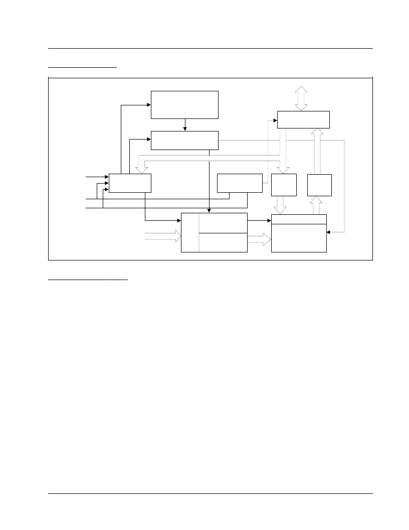
BLOCK DIAGRAM
DEVICE OPERATION
READ OPERATION
The access of Pm39F010/020/040 are similar to
EPROM. To read data, three control functions must be
satisfied:
CE# is the chip enable and should be pulled low
( V
IL
).
OE# is the output enable and should be pulled
low ( V
IL
).
WE# is the write enable and should remains high
( V
IH
)
.
PRODUCT IDENTIFICATION
The product identification mode can be used to identify
the manufacturer and the device through hardware or
software read ID operation. See Table 1 for PMC Manu-
facturer ID and Device ID. The hardware ID mode is acti-
vated by applying a 12.0 Volt on A9 pin, typically used
by an external programmer for selecting the right pro-
gramming algorithm for the devices. Refer to Table 2 for
Bus Operation Modes. The software ID mode is acti-
vated by a three-bus-cycle command. See Table 3 for
Software Command Definition.
WE#
CE#
OE#
COMMAND
REGISTER
CE,OE LOGIC
A0-A
MS
ERASE/PROGRAM
VOLTAGE
GENERATOR
HIGH VOLTAGE
SWITCH
I/O0-I/O7
I/O BUFFERS
DATA
LATCH
SENSE
AMP
Y-GATING
MEMORY
ARRAY
A
L
Y-DECODER
X-DECODER
BYTE PROGRAMMING
The programming is a four-bus-cycle operation and the
data is programmed into the devices (to a logical “0”) on
a byte-by-byte basis. See Table 3 for Software Com-
mand Definition. A program operation is activated by writ-
ing the three-byte command sequence followed by pro-
gram address and one byte of program data into the
devices. The addresses are latched on the falling edge
of WE# or CE# whichever occurs later, and the data are
latched on the rising edge of WE# or CE# whichever
occurs first. The internal control logic automatically
handles the internal programming voltages and timing.
A data “0” can not be programmed back to a “1”. Only
erase operation can convert the “0”s to “1”s. The Data#
Polling on I/O7 or Toggle Bit on I/O6 can be used to
detect the progress or completion of a program cycle.
相关PDF资料 |
PDF描述 |
|---|---|
| PM39F040-55VCE | 1 Mbit / 2 Mbit / 4 Mbit 5 Volt-only CMOS Flash Memory |
| PM39LV010 | 512 Kbit / 1Mbit / 2Mbit / 4Mbit 3.0 Volt-only CMOS Flash Memory |
| PM39LV010-70 | 512 Kbit / 1Mbit / 2Mbit / 4Mbit 3.0 Volt-only CMOS Flash Memory |
| PM39LV010-70JC | 512 Kbit / 1Mbit / 2Mbit / 4Mbit 3.0 Volt-only CMOS Flash Memory |
| PM39LV010-70JCE | 512 Kbit / 1Mbit / 2Mbit / 4Mbit 3.0 Volt-only CMOS Flash Memory |
相关代理商/技术参数 |
参数描述 |
|---|---|
| PM39F020-70JC | 制造商:PMC 制造商全称:PMC 功能描述:1 Mbit / 2 Mbit / 4 Mbit 5 Volt-only CMOS Flash Memory |
| PM39F020-70JCE | 制造商:PMC 制造商全称:PMC 功能描述:1 Mbit / 2 Mbit / 4 Mbit 5 Volt-only CMOS Flash Memory |
| PM39F020-70PC | 制造商:PMC 制造商全称:PMC 功能描述:1 Mbit / 2 Mbit / 4 Mbit 5 Volt-only CMOS Flash Memory |
| PM39F020-70PCE | 制造商:PMC 制造商全称:PMC 功能描述:1 Mbit / 2 Mbit / 4 Mbit 5 Volt-only CMOS Flash Memory |
| PM39F020-70VC | 制造商:PMC 制造商全称:PMC 功能描述:1 Mbit / 2 Mbit / 4 Mbit 5 Volt-only CMOS Flash Memory |
发布紧急采购,3分钟左右您将得到回复。