- 您现在的位置:买卖IC网 > PDF目录370013 > PP-MOD1V2 ISP INTERFACE MODULE PDF资料下载
参数资料
| 型号: | PP-MOD1V2 |
| 英文描述: | ISP INTERFACE MODULE |
| 中文描述: | ISP的接口模块 |
| 文件页数: | 24/48页 |
| 文件大小: | 3471K |
| 代理商: | PP-MOD1V2 |
第1页第2页第3页第4页第5页第6页第7页第8页第9页第10页第11页第12页第13页第14页第15页第16页第17页第18页第19页第20页第21页第22页第23页当前第24页第25页第26页第27页第28页第29页第30页第31页第32页第33页第34页第35页第36页第37页第38页第39页第40页第41页第42页第43页第44页第45页第46页第47页第48页
ISP Interface Module Version 1.00 27/06/01
17
4.9 J7 PPM ISP Connector
This connector provides the I/O interface between the
PPM and the PIM. The following groups of signals are
provided:
General purpose outputs
The SPI bus (MOSI, MISO, SCK)
Connections for three PPM “Status” LED’s
Target power supply +5V and a special negative
voltage output signal
General purpose Inputs (reserved for future use)
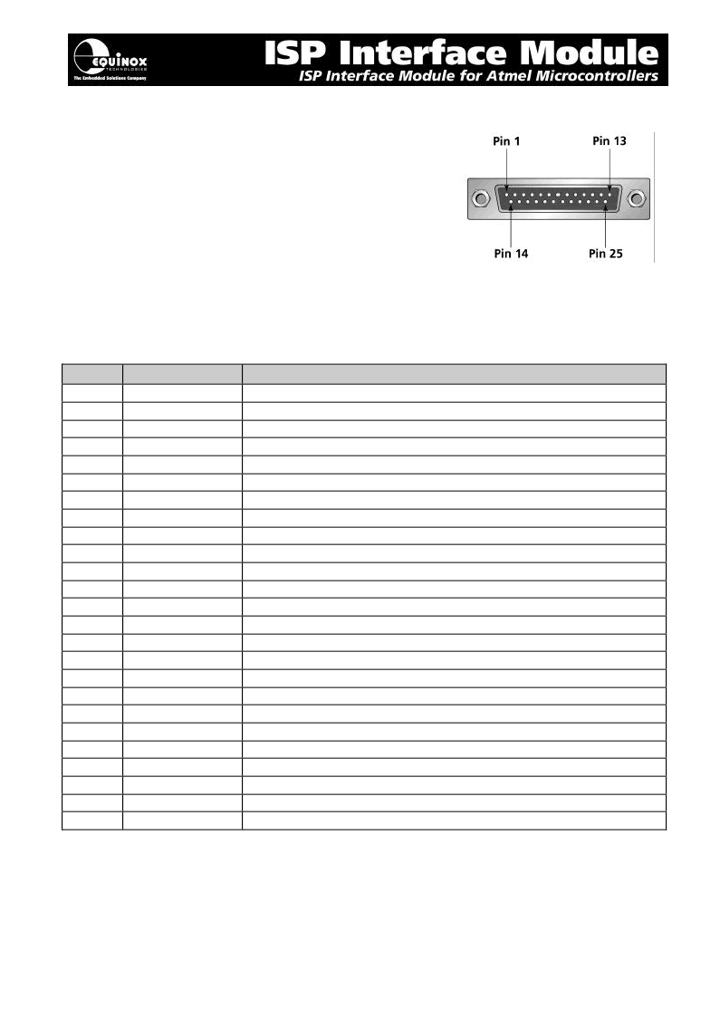
J1 Target Programming Connector - Pin out
Pin No Title
1
OP1_C
2
OP2_C
3
OP3_C
4
OP4_C (RESET)
5
MOSI_C
6
SCK_C
7
IP1_C
8
IP2_C
9
IP3_C
10
IP4_C
11
MISO_C
12
LED1A
13
LED1K
14
LED2A
15
LED2K
16
LED3A
17
LED3K
18
OP5
19
Vcc_OUT
20
Vcc_OUT
21
GND
22
SP1_IP
23
GND
24
Vcc
25
Vcc_TARGET_IN
Figure 34 – Target Programming
Connector (25-way Male D Connector)
Description
Output 1. Used to enable SCK2 generator U3
Output 2. Used to control VPP generator (Controls +12V RESET line)
Output 3. Used to control VPP generator (Vpp Output enable)
Output 4. Default RESET control signal
MOSI SPI signal. Master Out Slave In
SCK SPI signal. (Serial clock)
Input 1. Do not connect. Reserved for future use N/C
Input 2. Do not connect. Reserved for future use N/C
Input 3. Do not connect. Reserved for future use N/C
Input 4. Used with opto-isolator start
MISO SPI signal. Master In Slave Out
Anode of Busy LED (usually yellow)
Cathode of Busy LED (usually yellow)
Anode of Fault LED (usually red)
Cathode of Fault LED (usually red)
Anode of OK LED (usually green)
Cathode of OK LED (usually green)
Output 5. Negative voltage output signal. (-4.5V)
Vcc for target. Programmable voltage level
Vcc for target. Programmable voltage level
0V for target
Reserved for future use
0V for target
+5V
Target Vcc Voltage Input (Connects to J8 TV pin on PPM)
Figure 35
Please refer to the ‘PPM Programmer Module’ manual for further details
相关PDF资料 |
PDF描述 |
|---|---|
| PP01002 | GEHOERSCHUTZ OHRSTOEPSEL 250ST Inhalt pro Packung: 250 Stk. |
| PP0901SA | Direct ProTek Replacement:PP0901SA |
| PP0901SB | Direct ProTek Replacement:PP0901SB |
| PP1101SB | Direct ProTek Replacement:PP1101SB |
| PP1101SC | Direct ProTek Replacement:PP1101SC |
相关代理商/技术参数 |
参数描述 |
|---|---|
| PPM-PLS | 制造商:Panduit Corp 功能描述: |
| PPM-Q | 制造商:Panduit Corp 功能描述: |
| PPMR0004B | 功能描述:LABEL 30'X8" WHITE/GREEN 制造商:panduit corp 系列:- 包装:卷 零件状态:在售 类型:标签 标签类型:- 标签尺寸:- 材料:乙烯基 颜色:白色,绿色 配套使用产品/相关产品:- 标准包装:1 |
| PPMR0005B | 功能描述:LABEL 30'X8" WHITE/BLUE 制造商:panduit corp 系列:- 包装:卷 零件状态:在售 类型:标签 标签类型:- 标签尺寸:- 材料:乙烯基 颜色:白色,蓝色 配套使用产品/相关产品:- 标准包装:1 |
| PPMR0012B | 功能描述:ROLL PIPE MRKR,GAS8X30FT,8"X30FT 制造商:panduit corp 系列:- 包装:卷 零件状态:在售 类型:标签 标签类型:- 标签尺寸:- 材料:乙烯基 颜色:黑色,黄色 配套使用产品/相关产品:- 标准包装:1 |
发布紧急采购,3分钟左右您将得到回复。