- 您现在的位置:买卖IC网 > PDF目录268247 > PPC7448VS1400NC (FREESCALE SEMICONDUCTOR INC) 32-BIT, 1400 MHz, RISC PROCESSOR, CBGA360 PDF资料下载
参数资料
| 型号: | PPC7448VS1400NC |
| 厂商: | FREESCALE SEMICONDUCTOR INC |
| 元件分类: | 微控制器/微处理器 |
| 英文描述: | 32-BIT, 1400 MHz, RISC PROCESSOR, CBGA360 |
| 封装: | 25 X 25 MM, 2.20 MM HEIGHT, 1.27 MM PITCH, ROHS COMPLIANT, HCTE, CERAMIC, LGA-360 |
| 文件页数: | 11/14页 |
| 文件大小: | 134K |
| 代理商: | PPC7448VS1400NC |
MPC7448 Hardware Specifications Addendum for the MC7448xxnnnnNx Series, Rev. 6
6
Freescale Semiconductor
General Parameters
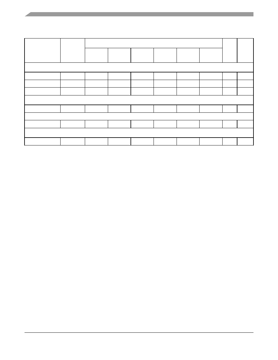
Table 7. Power Consumption for MPC7448 at Maximum Rated Frequency
Die
Junction
(Tj) (C)
C)
Maximum Processor Core Frequency (Speed Grade, MHz)
Unit
Notes
600,
667
800,
867
1000
1250
1267 7
1400
Full-Power Mode
Typical, Nominal
65
8.5
9.0
9.5
10.0
8.4
11.0
W
1, 2
Typical, Thermal
105
10.8
11.4
12.0
12.6
10.3
13.7
W
1, 5
Maximum
105
12.5
13.2
13.9
14.6
12.0
15.9
W
1, 3
Nap Mode
Typical
105
6.5
8.3
6.5
8.3
W
1, 6
Sleep Mode
Typical
105
6.3
8.0
6.3
8.0
W
1, 6
Deep Sleep Mode (PLL Disabled)
Typical
105
6.0
7.7
6.0
7.7
W
1, 6
Notes:
1. These values specify the power consumption for the core power supply (VDD) at nominal voltage and apply to all valid
processor bus frequencies and configurations. The values do not include I/O supply power (OVDD) or PLL supply power
(AVDD). OVDD power is system dependent but is typically < 5% of VDD power. Worst case power consumption for
AVDD <13mW.
2. Typical nominal power consumption is an average value measured at the nominal recommended VDD (see Table 4) and
65
°C while running the Dhrystone 2.1 benchmark and achieving 2.3 Dhrystone MIPs/MHz. This parameter is not 100%
tested but periodically sampled.
3. Maximum power consumption is the average measured at nominal VDD and maximum operating junction temperature (see
Table 4) while running an entirely cache-resident, contrived sequence of instructions to keep all the execution units
maximally busy.
4. Doze mode is not a user-definable state; it is an intermediate state between full-power and either nap or sleep mode. As a
result, power consumption for this mode is not tested.
5. Typical thermal power consumption is an average value measured at the nominal recommended VDD (see Table 4) and
105
°C while running the Dhrystone 2.1 benchmark and achieving 2.3 Dhrystone MIPs/MHz. This parameter is not 100%
tested but periodically sampled.
6. Typical power consumption for these modes is measured at the nominal recommended VDD (see Table 4) and 105°C in the
mode described. This parameter is not 100% tested but is periodically sampled.
7. Power consumption for the 1267 MHz device is intentionally constrained via testing and sorting to assure low power
consumption for this device.
相关PDF资料 |
PDF描述 |
|---|---|
| PIC16LF1936T-E/SP | 8-BIT, FLASH, 32 MHz, RISC MICROCONTROLLER, PDIP28 |
| PIC18LF24J10-E/SO | 8-BIT, FLASH, 40 MHz, RISC MICROCONTROLLER, PDSO28 |
| PIC16CR73-E/SP | 8-BIT, FLASH, 20 MHz, RISC MICROCONTROLLER, PDIP28 |
| PSD813F4-15JI | 128K X 8 FLASH, 27 I/O, PIA-GENERAL PURPOSE, PQCC52 |
| PSD813F4-15J | 128K X 8 FLASH, 27 I/O, PIA-GENERAL PURPOSE, PQCC52 |
相关代理商/技术参数 |
参数描述 |
|---|---|
| PPC7450RX600LD | 制造商:Freescale Semiconductor 功能描述: |
| PPC7457RX1000NB | 制造商:MOTOROLA 制造商全称:Motorola, Inc 功能描述:PPC7457RX1000NB |
| PPC7457RX600NB | 制造商:MOTOROLA 制造商全称:Motorola, Inc 功能描述:PPC7457RX1000NB |
| PPC7457RX733NB | 制造商:MOTOROLA 制造商全称:Motorola, Inc 功能描述:PPC7457RX1000NB |
| PPC7457RX867NB | 制造商:MOTOROLA 制造商全称:Motorola, Inc 功能描述:PPC7457RX1000NB |
发布紧急采购,3分钟左右您将得到回复。