- 您现在的位置:买卖IC网 > Datasheet目录633 > PS12014-A (Powerex Inc)MOD IPM 3PHASE IGBT 1200V 10A Datasheet资料下载
参数资料
| 型号: | PS12014-A |
| 厂商: | Powerex Inc |
| 文件页数: | 4/6页 |
| 文件大小: | 0K |
| 描述: | MOD IPM 3PHASE IGBT 1200V 10A |
| 标准包装: | 2 |
| 类型: | IGBT |
| 配置: | 三相反相器 |
| 电流: | 10A |
| 电压: | 1200V |
| 电压 - 隔离: | 2500Vrms |
| 封装/外壳: | 36-DIP 模块 |
�� �
�
�MITSUBISHI� SEMICONDUCTOR� <Application� Specific� Intelligent� Power� Module>�
�PS12014-A�
�FLAT-BASE� TYPE�
�INSULATED� TYPE�
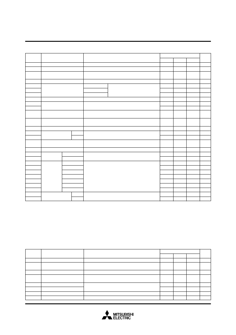
�ELECTRICAL� CHARACTERISTICS� (Tj� =� 25� °� C,� V� DH� =� 15V,� V� DB� =� 15V,� V� DL� =� 5V� unless� otherwise� noted)�
�Symbol�
�f� PWM�
�t� xx�
�t� dead�
�t� int�
�Item�
�PWM� input� frequency�
�Allowable� input� on-pulse� width�
�Allowable� input� signal� dead� time�
�for� blocking� arm� shoot-through�
�Input� inter-lock� sensing�
�Condition�
�T� C� ≤� 100� °� C,� Tj� ≤� 125� °� C�
�V� DH� =� 15V,� V� DL� =� 5V,� T� C� =� –20� °� C� ~� +100� °� C� Note� 3)�
�Relates� to� corresponding� inputs� (Except� brake� part)�
�T� C� =� –20� °� C� ~� +100� °� C�
�Relates� to� corresponding� inputs� (Except� brake� part)�
�Min.�
�2�
�2�
�4.0�
�—�
�Ratings�
�Typ.�
�—�
�—�
�—�
�65�
�Max.�
�15�
�500�
�—�
�100�
�Unit�
�kHz�
�μ� s�
�μ� s�
�ns�
�V� CO�
�Ic� =� 0A�
�V� DH� =� 15V�
�1.87�
�2.27�
�2.57�
�V�
�V� C+(200%)�
�V� C–(200%)�
�Analogue� signal� linearity� with�
�output� current�
�Ic� =� I� OP(200%)�
�Ic� =� –I� OP(200%)�
�V� DL� =� 5V�
�T� C� =� –20� ~� 100� °� C�
�(Fig.4)�
�0.77�
�2.97�
�1.17�
�3.37�
�1.47�
�3.67�
�V�
�V�
�|� ?� V� CO� |�
�Offset� change� area� vs� temperature� V� DH� =� 15V,� V� DL� =� 5V,� T� C� =� –20� ~� 100� °� C�
�—�
�15�
�—�
�mV�
�V� C+�
�V� C–�
�Analogue� signal� output� voltage� limit�
�Ic� >� I� OP(200%)� ,� V� DH� =� 15V,�
�V� DL� =� 5V�
�(Fig.� 4)�
�—�
�4.0�
�—�
�—�
�0.7�
�—�
�V�
�V�
�?� V� C� (200%)�
�r� CH�
�Analogue� signal� overall� linear�
�variation�
�Analogue� signal� data� hold�
�accuracy�
�|V� CO� -V� C� ±� (200%)� |�
�Correspond� to� max.� 500� μ� s� data� hold� period� only,�
�Ic� =� I� OP(200%)� (Fig.� 5)�
�—�
�–5�
�1.1�
�—�
�—�
�5�
�V�
�%�
�t� d(read)�
�Analogue� signal� reading� time�
�After� input� signal� trigger� point�
�(Fig.� 8)�
�—�
�3�
�—�
�μ� s�
�I� CL(H)�
�I� CL(L)�
�Signal� output� cur-�
�rent� of� CL� operation�
�Idle�
�Active�
�Open� collector� onput�
�—�
�—�
�—�
�1�
�1�
�—�
�μ� A�
�mA�
�±� I� OL�
�CL� warning� operation� level�
�V� DL� =� 5V,� V� DH� =� 15V,� T� C� =� –20� ~� 100� °� C�
�(Note� 4)�
�9.14�
�11.05�
�13.90�
�A�
�SC�
�Short� circuit� current� trip� level�
�Tj� =� 25� °� C�
�(Fig.� 7),� (Note� 5)�
�15.30�
�26.80�
�38.90�
�A�
�OT�
�OTr�
�UV� DB�
�UV� DBr�
�UV� DH�
�UV� DHr�
�OV� DH�
�OV� DHr�
�t� dv�
�Over� tenperature�
�protection�
�Supply� circuit�
�under� and�
�over� voltage�
�protection�
�Trip� level�
�Reset� level�
�Trip� level�
�Reset� level�
�Trip� level�
�Reset� level�
�Trip� level�
�Reset� level�
�Filter� time�
�V� DL� =� 5V,� V� DH� =� 15V�
�T� C� =� –20� °� C� ~� +100� °� C�
�Tj� ≤� 125� °� C�
�100�
�—�
�10.0�
�10.5�
�11.05�
�11.55�
�18.00�
�16.50�
�—�
�110�
�90�
�11.0�
�11.5�
�12.00�
�12.50�
�19.20�
�17.50�
�10�
�120�
�—�
�12.0�
�12.5�
�12.75�
�13.25�
�20.15�
�18.65�
�—�
�°� C�
�°� C�
�V�
�V�
�V�
�V�
�V�
�V�
�μ� s�
�I� FO(H)�
�I� FO(L)�
�Fault� output� current�
�Idle�
�Active�
�Open� collector� output�
�—�
�—�
�—�
�1�
�1�
�—�
�μ� A�
�mA�
�(Note� 3)� :� (a)� Allowable� minimum� input� on-pulse� width� :� This� item� applies� to� P-side� circuit� only.�
�(b)� Allowable� maximum� input� on-pulse� width� :� This� item� applies� to� both� P-side� and� N-side� circuits� excluding� the� brake� circuit.�
�(Note4)� :� CL� output� :� The� "current� limit� warning� (CL)� operation� circuit� outputs� warning� signal� whenever� the� arm� current� exceeds� this� limit.� The�
�circuit� is� reset� automatically� by� the� next� input� signal� and� thus,� it� operates� on� a� pulse-by-pulse� scheme.�
�(Note5)� :� The� short� circuit� protection� works� instantaneously� when� a� high� short� circuit� current� flows� through� an� internal� IGBT� rising� up� momen-�
�tarily.� The� protection� function� is,� thus� meant� primarily� to� protect� the� ASIPM� against� short� circuit� distraction.� Therefore,� this� function� is�
�not� recommended� to� be� used� for� any� system� load� current� regulation� or� any� over� load� control� as� this� might,� cause� a� failure� due� to�
�excessive� temperature� rise.� Instead,� the� analogue� current� output� feature� or� the� over� load� warning� feature� (CL)� should� be� appropri-�
�ately� used� for� such� current� regulation� or� over� load� control� operation.� In� other� words,� the� PWM� signals� to� the� ASIPM� should� be� shut�
�down,� in� principle,� and� not� to� be� restarted� before� the� junction� temperature� would� recover� to� normal,� as� soon� as� a� fault� is� feed� back�
�from� its� F� O1� pin� of� the� ASIPM� indicating� a� short� circuit� situation.�
�RECOMMENDED� CONDITIONS�
�Symbol�
�V� CC�
�V� DH� ,� V� DB�
�V� DL�
�?� V� DH� ,� ?� V� DB� ,�
�?� V� DL�
�V� CIN(on)�
�V� CIN(off)�
�f� PWM�
�t� dead�
�Item�
�Supply� voltage�
�Control� supply� voltage�
�Control� supply� voltage�
�Supply� voltage� ripple�
�Input� ON� voltage�
�Input� OFF� voltage�
�PWM� Input� frequency�
�Arm� shoot-through� blocking� time�
�Condition�
�Applied� between� P-N�
�Applied� between� V� DH� -GND,� C� BU+� -C� BU–� ,� C� BV+� -C� BV–� ,�
�C� BW+� -C� BW–�
�Applied� between� V� DL� -GND�
�Using� application� circuit�
�Using� application� circuit�
�Min.�
�—�
�13.5�
�4.8�
�–1�
�—�
�4.8�
�2�
�4.0�
�Ratings�
�Typ.�
�600�
�15.0�
�5.0�
�—�
�—�
�—�
�10�
�—�
�Max.�
�800�
�16.5�
�5.2�
�+1�
�0.3�
�—�
�15�
�—�
�Unit�
�V�
�V�
�V�
�V/� μ� s�
�V�
�V�
�kHz�
�μ� s�
�Jan.� 2000�
�相关PDF资料 |
PDF描述 |
|---|---|
| PS12015-A | MOD IPM 3PHASE IGBT 1200V 15A |
| PS12017-A | MOD IPM 3PHASE IGBT 1200V 25A |
| PS12018-A | MOD IPM 3PHASE IGBT 1200V 25A |
| PS12032 | MOD IPM 3PHASE IGBT 1200V 5A |
| PS12033 | MOD IPM 3PHASE IGBT 1200V 5A |
相关代理商/技术参数 |
参数描述 |
|---|---|
| PS12015 | 制造商:POWEREX 制造商全称:Powerex Power Semiconductors 功能描述:FLAT-BASE TYPE INSULATED TYPE |
| PS120-15 | 制造商:Banner Engineering 功能描述:Power Supply, 120VAC Input, 15VDC @ 1 Amp Output, 8 Pin Octal Socket Connection |
| PS12015-A | 功能描述:MOD IPM 3PHASE IGBT 1200V 15A RoHS:否 类别:半导体模块 >> 功率驱动器 系列:- 标准包装:15 系列:SPM® 类型:FET 配置:三相反相器 电流:1.8A 电压:500V 电压 - 隔离:1500Vrms 封装/外壳:23-DIP 模块 |
| PS12017-A | 功能描述:MOD IPM 3PHASE IGBT 1200V 25A RoHS:否 类别:半导体模块 >> 功率驱动器 系列:- 标准包装:15 系列:SPM® 类型:FET 配置:三相反相器 电流:1.8A 电压:500V 电压 - 隔离:1500Vrms 封装/外壳:23-DIP 模块 |
| PS12018-A | 功能描述:MOD IPM 3PHASE IGBT 1200V 25A RoHS:否 类别:半导体模块 >> 功率驱动器 系列:- 标准包装:15 系列:SPM® 类型:FET 配置:三相反相器 电流:1.8A 电压:500V 电压 - 隔离:1500Vrms 封装/外壳:23-DIP 模块 |
发布紧急采购,3分钟左右您将得到回复。