- 您现在的位置:买卖IC网 > PDF目录65979 > PS21353-G AC MOTOR CONTROLLER, 20 A, DMA35 PDF资料下载
参数资料
| 型号: | PS21353-G |
| 元件分类: | 运动控制电子 |
| 英文描述: | AC MOTOR CONTROLLER, 20 A, DMA35 |
| 文件页数: | 2/9页 |
| 文件大小: | 153K |
| 代理商: | PS21353-G |
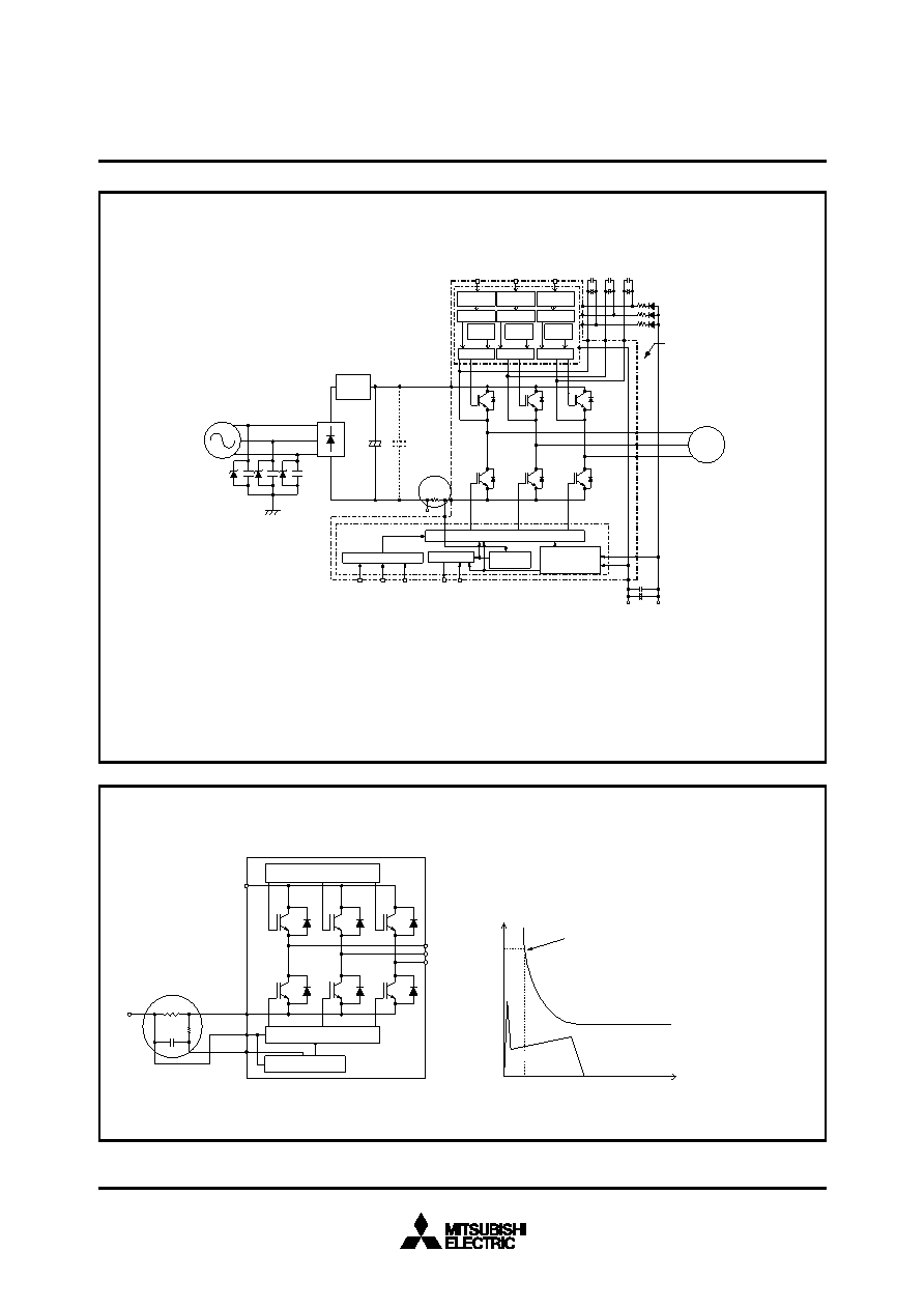
MITSUBISHI SEMICONDUCTOR <Intelligent Power Module>
PS21353-G
TRANSFER-MOLD TYPE
INSULATED TYPE
Sep. 2001
Z
Drive circuit
CBU–
CBU+
CBV–
CBV+
CBW–
CBW+
(15V line)
(5V line)
(Note 1, 2)
VD
VNC
W
AC input
AC line output
V
U
Input signal
coditioning
Level shifter
Drive circuit
Protection
circuit (UV)
Input signal
coditioning
Input signal
coditioning
Input signal conditioning
Fo logic
SC
protection
Protection
circuit (UV)
Protection
circuit (UV)
Control supply
Under-Voltage
protection
Drive circuit Drive circuit
FO
CFO
P
N1
N
FO output (5V line)
(Note 3, 5)
High-side input (PWM)
(5V line)
(Note 1,2)
Low-side input (PWM)
M
(Note 6)
DIP-IPM
C
C4
C3
C3 : Tight tolerance, temp-compensated electrolytic type
C4 : 0.22~2
F R-category ceramic capacitor for noise filtering.
(Note : The capacitance value depends on the PWM control
scheme used in the applied system).
Note1:
To prevent the input signals oscillation, an RC coupling at each input is recommended. (see also Fig. 6)
2:
By virtue of integrating an application specific type HVIC inside the module, direct coupling to CPU terminals without any opto-coupler or transformer
isolation is possible. (see also Fig. 6)
3:
This output is open collector type. The signal line should be pulled up to the positive side of the 5V power supply with approximately 5.1k
resistance.
(see also Fig. 6)
4:
The wiring between the power DC link capacitor and the P/N1 terminals should be as short as possible to protect the DIP-IPM against catastrophic high
surge voltages. For extra precaution, a small film type snubber capacitor (0.1~0.22
F, high voltage type) is recommended to be mounted close to
these P and N1 DC power input terminals.
5:
Fo output pulse width should be decided by connecting external capacitor between CFO and VNC terminals. (Example : CFO=22nF
→ tFO=1.8ms (Typ.))
6:
High voltage (600V or more) and fast recovery type (less than 100ns) diodes should be used in the bootstrap circuit.
H-side IGBTS
L-side IGBTS
CIN
(Note 4)
Fig. 3
Inrush current
limiter circuit
Level shifter Level shifter
Z : ZNR (Surge absorber)
C : AC filter (Ceramic capacitor 2.2~6.5nF)
(Note : Additionally, an appropriate line to line
surge absorber circuit may become necessary
depending on the application environment.)
Note1: In the recommended external protection circuit, please select the RC time constant in the range 1.5~2.0
s.
2: To prevent erroneous protection operation, the wiring of A, B, C should be as short as possible.
Drive circuit
Protection circuit
W
V
U
B
C
VNC
CIN
A
P
N1
N
C
R
Shunt Resistor
External protection circuit
DIP-IPM
L-side IGBTS
H-side IGBTS
SC Protection
Trip Level
IC (A)
tw (
s)
2
0
Short Circuit Protective Function (SC) :
SC protection is achieved by sensing the L-side DC-Bus current (through the external
shunt resistor) after allowing a suitable filtering time (defined by the RC circuit).
When the sensed shunt voltage exceeds the SC trip-level, all the L-side IGBTs are turned
OFF and a fault signal (Fo) is output. Since the SC fault may be repetitive, it is
recommended to stop the system when the Fo signal is received and check the fault.
Collector current
waveform
(Note 1)
(Note 2)
Fig. 2 INTERNAL FUNCTIONS BLOCK DIAGRAM (TYPICAL APPLICATION EXAMPLE)
Fig. 3 EXTERNAL PART OF THE DIP-IPM PROTECTION CIRCUIT
相关PDF资料 |
PDF描述 |
|---|---|
| PS21353-N | AC MOTOR CONTROLLER, 20 A, DMA35 |
| PS21454-E | AC MOTOR CONTROLLER, 30 A, DMA26 |
| PS21562-S | AC MOTOR CONTROLLER, 10 A, XMA37 |
| PS21661-FR | AC MOTOR CONTROLLER, 6 A, XMA35 |
| PS21661-RZ | AC MOTOR CONTROLLER, 6 A, XMA35 |
相关代理商/技术参数 |
参数描述 |
|---|---|
| PS21353GP | 制造商:POWEREX 制造商全称:Powerex Power Semiconductors 功能描述:Intellimoda?¢ Module |
| PS21353-GP | 功能描述:MOD IPM 600V 10A MINI-DIP RoHS:是 类别:半导体模块 >> 功率驱动器 系列:Intellimod™ 标准包装:15 系列:SPM® 类型:FET 配置:三相反相器 电流:1.8A 电压:500V 电压 - 隔离:1500Vrms 封装/外壳:23-DIP 模块 |
| PS21353-N | 制造商:MITSUBISHI 制造商全称:Mitsubishi Electric Semiconductor 功能描述:600V/10A low-loss 4th generation (planar) IGBT inverter bridge for 3 phase DC-to-AC power conversion. |
| PS21353-NP | 制造商:MITSUBISHI 制造商全称:Mitsubishi Electric Semiconductor 功能描述:Generation DIP and Mini-DIP-IPM |
| PS214 | 制造商:未知厂家 制造商全称:未知厂家 功能描述:Analog IC |
发布紧急采购,3分钟左右您将得到回复。