- 您现在的位置:买卖IC网 > PDF目录65979 > PS21961-AT AC MOTOR CONTROLLER, 6 A, DMA25 PDF资料下载
参数资料
| 型号: | PS21961-AT |
| 元件分类: | 运动控制电子 |
| 英文描述: | AC MOTOR CONTROLLER, 6 A, DMA25 |
| 封装: | DIP-25 |
| 文件页数: | 6/7页 |
| 文件大小: | 176K |
| 代理商: | PS21961-AT |
MITSUBISHI SEMICONDUCTOR <Dual-In-Line Package Intelligent Power Module>
PS21961-T/-AT/-CT/-TW
TRANSFER-MOLD TYPE
INSULATED TYPE
Mar. 2009
6
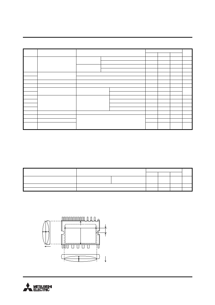
Note 8: Flatness measurement position
+–
+
–
Heat sink side
4.6mm
Measurement position
Mounting screw : M3
(Note 7)
Condition
Parameter
Limits
Mounting torque
Weight
Heat-sink flatness
Min.
MECHANICAL CHARACTERISTICS AND RATINGS
Typ.
Max.
0.59
—
–50
Unit
—
10
—
0.78
—
100
Nm
g
m
Recommended : 0.69 Nm
(Note 8)
Note 7 : Plain washers (ISO 7089~7094) are recommended.
CONTROL (PROTECTION) PART
Note 4 : Short circuit protection is functioning only for the lower-arms. Please select the external shunt resistance such that the SC trip-level is
less than 1.7 times of the current rating.
5: Over temperature protection (OT) outputs fault signal, when the LVIC temperature exceeds OT trip temperature level (OTt). In that case
if the heat sink comes off DIPIPM or fixed loosely, don’t reuse that DIPIPM. (There is a possibility that junction temperature of power chips
exceeded maximum Tj (150
°C)).
6: Fault signal is asserted only corresponding to a SC, a UV or an OT failure at lower side, and the FO pulse width is different for each fail-
ure modes. For SC failure, FO output is with a fixed width of 20
sec(min), but for UV or OT failure, FO output continuously during the
whole UV or OT period, however, the minimum FO pulse width is 20
sec(min) for very short UV or OT period less than 20sec.
Symbol
ID
VFOH
VFOL
VSC(ref)
IIN
OTt
OTrh
UVDBt
UVDBr
UVDt
UVDr
tFO
Vth(on)
Vth(off)
Vth(hys)
Parameter
Condition
Limits
Unit
Circuit current
Fault output voltage
Short circuit trip level
Control supply under-voltage
protection
Fault output pulse width
ON threshold voltage
OFF threshold voltage
ON/OFF threshold hysteresis
voltage
VD = VDB = 15V
VIN = 5V
Total of VP1-VNC, VN1-VNC
VUFB-U, VVFB-V, VWFB-W
VSC = 0V, FO terminal pull-up to 5V by 10k
VSC = 1V, IFO = 1mA
Tj = 25
°C, VD = 15V
(Note 4)
VIN = 5V
Trip level
Trip/reset hysteresis
Trip level
Reset level
Trip level
Reset level
(Note 6)
Applied between UP, VP, WP, UN, VN, WN-VNC
—
4.9
—
0.43
0.70
100
—
10.0
10.5
10.3
10.8
20
—
0.8
0.35
—
0.48
1.00
120
10
—
2.1
1.3
0.65
2.80
0.55
2.80
0.55
—
0.95
0.53
1.50
140
—
12.0
12.5
13.0
—
2.6
—
Min.
Typ.
Max.
mA
V
mA
°C
V
s
V
VD = VDB = 15V
VIN = 0V
Total of VP1-VNC, VN1-VNC
VUFB-U, VVFB-V, VWFB-W
Tj
≤ 125°C
Input current
Over temperature protection
(Note 5)
VD = 15V,
At temperature of LVIC
相关PDF资料 |
PDF描述 |
|---|---|
| PS21963-4ES | AC MOTOR CONTROLLER, DMA25 |
| PS21963-4E | AC MOTOR CONTROLLER, 16 A, DMA24 |
| PS21963-4S | AC MOTOR CONTROLLER, 20 A, DMA24 |
| PS21964-4A | AC MOTOR CONTROLLER, 30 A, DMA24 |
| PS21964-4C | AC MOTOR CONTROLLER, 30 A, DMA24 |
相关代理商/技术参数 |
参数描述 |
|---|---|
| PS21961-C | 制造商:POWEREX 制造商全称:Powerex Power Semiconductors 功能描述:Dual-In-Line Intelligent Power Module 3 Amperes/600 Volts |
| PS21961-CT | 制造商:MITSUBISHI 制造商全称:Mitsubishi Electric Semiconductor 功能描述:Dual-In-Line Package Intelligent Power Module TRANSFER-MOLD TYPE INSULATED TYPE |
| PS21961-ST | 制造商:MITSUBISHI 制造商全称:Mitsubishi Electric Semiconductor 功能描述:Dual-In-Line Package Intelligent Power Module TRANSFER-MOLD TYPE INSULATED TYPE |
| PS21961-T | 制造商:MITSUBISHI 制造商全称:Mitsubishi Electric Semiconductor 功能描述:Dual-In-Line Package Intelligent Power Module TRANSFER-MOLD TYPE INSULATED TYPE |
| PS21961-TW | 制造商:MITSUBISHI 制造商全称:Mitsubishi Electric Semiconductor 功能描述:Dual-In-Line Package Intelligent Power Module TRANSFER-MOLD TYPE INSULATED TYPE |
发布紧急采购,3分钟左右您将得到回复。