- 您现在的位置:买卖IC网 > PDF目录296863 > PSD4235F1V-12B81I (意法半导体) Flash In-System-Programmable Peripherals for 16-Bit MCUs PDF资料下载
参数资料
| 型号: | PSD4235F1V-12B81I |
| 厂商: | 意法半导体 |
| 英文描述: | Flash In-System-Programmable Peripherals for 16-Bit MCUs |
| 中文描述: | Flash在系统可编程外设的16位微控制器 |
| 文件页数: | 49/93页 |
| 文件大小: | 503K |
| 代理商: | PSD4235F1V-12B81I |
第1页第2页第3页第4页第5页第6页第7页第8页第9页第10页第11页第12页第13页第14页第15页第16页第17页第18页第19页第20页第21页第22页第23页第24页第25页第26页第27页第28页第29页第30页第31页第32页第33页第34页第35页第36页第37页第38页第39页第40页第41页第42页第43页第44页第45页第46页第47页第48页当前第49页第50页第51页第52页第53页第54页第55页第56页第57页第58页第59页第60页第61页第62页第63页第64页第65页第66页第67页第68页第69页第70页第71页第72页第73页第74页第75页第76页第77页第78页第79页第80页第81页第82页第83页第84页第85页第86页第87页第88页第89页第90页第91页第92页第93页
PSD4000 Series
Preliminary Information
50
9.4.3 Port Configuration Registers (PCRs)
Each port has a set of PCRs used for configuration. The contents of the registers can be
accessed by the microcontroller through normal read/write bus cycles at the addresses
given in Table 6. The addresses in Table 6 are the offsets in hex from the base of the
CSIOP register.
The pins of a port are individually configurable and each bit in the register controls its
respective pin. For example, Bit 0 in a register refers to Bit 0 of its port. The three PCRs,
shown in Table 19, are used for setting the port configurations. The default power-up state
for each register in Table 22 is 00h.
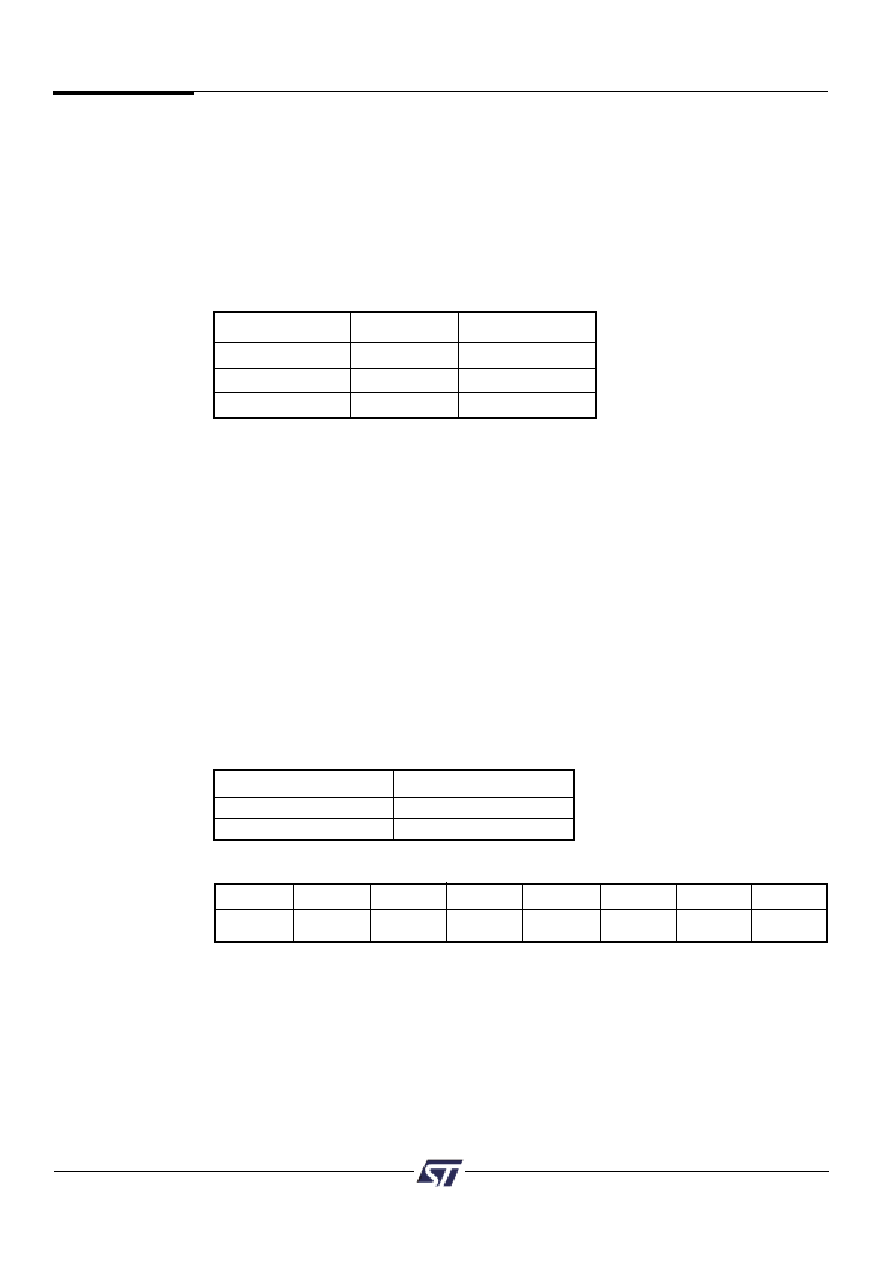
Register Name
Port
MCU Access
Control
E,F,G
Write/Read
Direction
A,B,C,D,E,F,G
Write/Read
Drive Select*
A,B,C,D,E,F,G
Write/Read
Table 19. Port Configuration Registers
*NOTE: See Table 22 for Drive Register bit definition.
The
PSD4000
Functional
Blocks
(cont.)
9.4.3.1 Control Register
Any bit set to ‘0’ in the Control Register sets the corresponding Port pin to MCU I/O Mode,
and a ‘1’ sets it to Address Out Mode. The default mode is MCU I/O. Only Ports E, F and
G have an associated Control Register.
9.4.3.2 Direction Register
The Direction Register controls the direction of data flow in the I/O Ports. Any bit set to ‘1’
in the Direction Register will cause the corresponding pin to be an output, and any bit set
to ‘0’ will cause it to be an input. The default mode for all port pins is input.
Figures 21 and 23 show the Port Architecture diagrams for Ports A/B/C and E/F/G
respectively. The direction of data flow for Ports A, B, C and F are controlled by the
direction register.
An example of a configuration for a port with the three least significant bits set to output
and the remainder set to input is shown in Table 21. Since Port D only contains four pins,
the Direction Register for Port D has only the four least significant bits active.
Direction Register Bit
Port Pin Mode
0
Input
1
Output
Table 20. Port Pin Direction Control
Bit 7
Bit 6
Bit 5
Bit 4
Bit 3
Bit 2
Bit 1
Bit 0
0
000
0
1
Table 21. Port Direction Assignment Example
相关PDF资料 |
PDF描述 |
|---|---|
| PSD4235F1V-12J | Flash In-System-Programmable Peripherals for 16-Bit MCUs |
| PSD4235F1V-12JI | Flash In-System-Programmable Peripherals for 16-Bit MCUs |
| PSD4235F1V-12M | MGrid IDT Rec /OPolKeyLRmp .38AuLF 40Ckt |
| PSD4235F2V-12B81I | Flash In-System-Programmable Peripherals for 16-Bit MCUs |
| PSD835F1V-12B81 | Configurable Memory System on a Chip for 8-Bit Microcontrollers |
相关代理商/技术参数 |
参数描述 |
|---|---|
| PSD4235G2-70U | 功能描述:SPLD - 简单可编程逻辑器件 5.0V 4M 70ns RoHS:否 制造商:Texas Instruments 逻辑系列:TICPAL22V10Z 大电池数量:10 最大工作频率:66 MHz 延迟时间:25 ns 工作电源电压:4.75 V to 5.25 V 电源电流:100 uA 最大工作温度:+ 75 C 最小工作温度:0 C 安装风格:Through Hole 封装 / 箱体:DIP-24 |
| PSD4235G2-90U | 功能描述:CPLD - 复杂可编程逻辑器件 5.0V 4M 90ns RoHS:否 制造商:Lattice 系列: 存储类型:EEPROM 大电池数量:128 最大工作频率:333 MHz 延迟时间:2.7 ns 可编程输入/输出端数量:64 工作电源电压:3.3 V 最大工作温度:+ 90 C 最小工作温度:0 C 封装 / 箱体:TQFP-100 |
| PSD4235G2-90UI | 功能描述:CPLD - 复杂可编程逻辑器件 5.0V 4M 90ns RoHS:否 制造商:Lattice 系列: 存储类型:EEPROM 大电池数量:128 最大工作频率:333 MHz 延迟时间:2.7 ns 可编程输入/输出端数量:64 工作电源电压:3.3 V 最大工作温度:+ 90 C 最小工作温度:0 C 封装 / 箱体:TQFP-100 |
| PSD4235G2V-12UI | 功能描述:CPLD - 复杂可编程逻辑器件 3.3V 4M 120ns RoHS:否 制造商:Lattice 系列: 存储类型:EEPROM 大电池数量:128 最大工作频率:333 MHz 延迟时间:2.7 ns 可编程输入/输出端数量:64 工作电源电压:3.3 V 最大工作温度:+ 90 C 最小工作温度:0 C 封装 / 箱体:TQFP-100 |
| PSD4235G2V-90U | 功能描述:CPLD - 复杂可编程逻辑器件 3.3V 4M 90ns RoHS:否 制造商:Lattice 系列: 存储类型:EEPROM 大电池数量:128 最大工作频率:333 MHz 延迟时间:2.7 ns 可编程输入/输出端数量:64 工作电源电压:3.3 V 最大工作温度:+ 90 C 最小工作温度:0 C 封装 / 箱体:TQFP-100 |
发布紧急采购,3分钟左右您将得到回复。