- 您现在的位置:买卖IC网 > PDF目录224799 > PSD4235G2V-A-15UI (意法半导体) Flash In-System-Programmable Peripherals for 16-Bit MCUs PDF资料下载
参数资料
| 型号: | PSD4235G2V-A-15UI |
| 厂商: | 意法半导体 |
| 英文描述: | Flash In-System-Programmable Peripherals for 16-Bit MCUs |
| 中文描述: | Flash在系统可编程外设的16位微控制器 |
| 文件页数: | 13/93页 |
| 文件大小: | 503K |
| 代理商: | PSD4235G2V-A-15UI |
第1页第2页第3页第4页第5页第6页第7页第8页第9页第10页第11页第12页当前第13页第14页第15页第16页第17页第18页第19页第20页第21页第22页第23页第24页第25页第26页第27页第28页第29页第30页第31页第32页第33页第34页第35页第36页第37页第38页第39页第40页第41页第42页第43页第44页第45页第46页第47页第48页第49页第50页第51页第52页第53页第54页第55页第56页第57页第58页第59页第60页第61页第62页第63页第64页第65页第66页第67页第68页第69页第70页第71页第72页第73页第74页第75页第76页第77页第78页第79页第80页第81页第82页第83页第84页第85页第86页第87页第88页第89页第90页第91页第92页第93页
Preliminary Information
PSD4000 Series
17
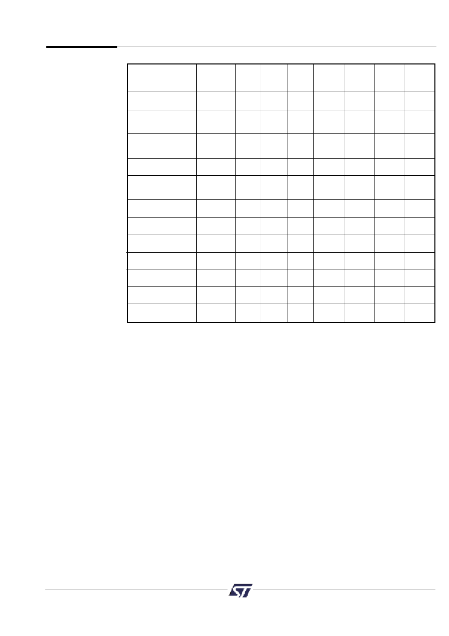
FS0-7
Instruction
or
(Note 14)
CSBOOT0-3 Cycle 1 Cycle 2 Cycle 3
Cycle 4
Cycle5
Cycle 6
Cycle 7
Read (Note 5)
1
“Read”
RA RD
Read Main Flash ID
1
AAh
55h
90h
“Read”
(Note 6)
@XAAAh @X554h @XAAAh
ID
@XX02h
Read Sector Protection
1
AAh
55h
90h
“Read”
(Notes 6,8,13)
@XAAAh @X554h @XAAAh 00h or 01h
@XX04h
Program a Flash Word
1
AAh
55h
A0h
PD@PA
@XAAAh @X554h @XAAAh
Erase One Flash Sector
1
AAh
55h
80h
AAh
55h
30h
@XAAAh @X554h @XAAAh
@XAAAh
@X554h
@SA
@next SA
(Note 7)
Erase Flash Block
1
AAh
55h
80h
AAh
55h
10h
(Bulk Erase)
@XAAAh @X554h @XAAAh
@XAAAh
@X554h
@XAAAh
Suspend Sector Erase
1
B0h
(Note 11)
@xxxh
Resume Sector Erase
1
30h
(Note 12)
@xxxh
Reset (Note 6)
1
F0 @ any
address
Unlock Bypass
1
AAh
55h
20h
@XAAAh @X554h @XAAAh
Unlock Bypass Program
1
A0h
PD@PA
(Note 9)
@XXXXh
Unlock Bypass Reset
1
90h
00h
(Note 10)
@XXXXh @XXXXh
Table 8. Instructions
X
= Don’t Care. “xxxh” address in the above table must be an even address.
RA = Address of the memory location to be read.
RD = Data read from location RA during read operation.
PA = Address of the memory location to be programmed. Addresses are latched on the falling edge of the WR#
(CNTL0) pulse. PA is an even address for PSD in word programming mode.
PD = Data (word) to be programmed at location PA. Data is latched on the rising edge of WR# (CNTL0) pulse.
SA = Address of the sector to be erased or verified. The chip select (FS0-7 or CSBOOT0-3) of the sector to be
erased must be active (high).
NOTES:
1.
All bus cycles are write bus cycle except the ones with the “read” label.
2.
All values are in hexadecimal.
3.
FS0-7 and CSBOOT0-3 are active high and are defined in PSDsoft.
4.
Only Address bits A11-A0 are used in Instruction decoding.
5.
No unlock or command cycles required when device is in read mode.
6.
The Reset command is required to return to the read mode after reading the Flash ID, Sector Protect status
or if DQ5 (DQ13) goes high.
7.
Additional sectors to be erased must be entered within 80s.
8.
The data is 00h for an unprotected sector and 01h for a protected sector. In the fourth cycle, the sector chip
select is active and (A1 = 1, A0 = 0).
9.
The Unlock Bypass command is required prior to the Unlock Bypass Program command.
10. The Unlock Bypass Reset command is required to return to reading array data when the device is in the
Unlock Bypass mode.
11. The system may read and program functions in non-erasing sectors, read the Flash ID or read the Sector
Protect status, when in the Erase Suspend mode. The erase Suspend command is valid only during a sector
erase operation.
12. The Erase Resume command is valid only during the Erase Suspend mode.
13. The MCU cannot invoke these instructions while executing code from the same Flash memory for which the
instruction is intended. The MCU must fetch, for example, codes from the Secondary Flash memory when
reading the Sector Protection Status of the main Flash.
14. All write bus cycles in an instruction are byte write to even address (XA4Ah or X554h). Flash Programming
bys cycle is writing a word to even address.
The
PSD4000
Functional
Blocks
(cont.)
相关PDF资料 |
PDF描述 |
|---|---|
| PSD4235G2V-A-20B81 | Tantalum Electrolytic Capacitor; Capacitance:100uF; Capacitance Tolerance:+/- 20 %; Working Voltage, DC:10V; Package/Case:7343-31; Terminal Type:PCB SMT; ESR:0.0055ohm; Dielectric Material:Tantalum; Operating Temp. Max:105 C |
| PSD4235G2V-A-20B81I | Flash In-System-Programmable Peripherals for 16-Bit MCUs |
| PSD4235G2V-A-70M | Conductive Polymer Chip Capacitors / T520 Series - KO Cap; Capacitance [nom]: 150uF; Working Voltage (Vdc)[max]: 6.3V; Capacitance Tolerance: +/-20%; Dielectric: Conductive Polymer; ESR: 15mΩ; Lead Style: Surface-Mount Chip; Lead Dimensions: 7343-31; Termination: 100% Tin (Sn); Body Dimensions: 7.3mm x 4.3mm x 2.8mm; Temperature Range: -55C to +105C; Container: Tape & Reel; Qty per Container: 500; Features: Low ESR |
| PSD4235G2V-A-70MI | Flash In-System-Programmable Peripherals for 16-Bit MCUs |
| PSD4235G2V-A-70U | Flash In-System-Programmable Peripherals for 16-Bit MCUs |
相关代理商/技术参数 |
参数描述 |
|---|---|
| PSD4256G6V-10UI | 功能描述:CPLD - 复杂可编程逻辑器件 3.3V 8M 100ns RoHS:否 制造商:Lattice 系列: 存储类型:EEPROM 大电池数量:128 最大工作频率:333 MHz 延迟时间:2.7 ns 可编程输入/输出端数量:64 工作电源电压:3.3 V 最大工作温度:+ 90 C 最小工作温度:0 C 封装 / 箱体:TQFP-100 |
| PSD4-36 | 制造商:Tamura Corporation of America 功能描述: |
| PSD-45 | 制造商:MEANWELL 制造商全称:Mean Well Enterprises Co., Ltd. 功能描述:45W DC-DC Single Output Switching Power Supply |
| PSD-45_11 | 制造商:MEANWELL 制造商全称:Mean Well Enterprises Co., Ltd. 功能描述:45W DC-DC Single Output Switching Power Supply |
| PSD-45A-05 | 功能描述:线性和开关式电源 30W 5Vout 6A Input 9.2-18VDC RoHS:否 制造商:TDK-Lambda 产品:Switching Supplies 开放式框架/封闭式:Enclosed 输出功率额定值:800 W 输入电压:85 VAC to 265 VAC 输出端数量:1 输出电压(通道 1):20 V 输出电流(通道 1):40 A 商用/医用: 输出电压(通道 2): 输出电流(通道 2): 安装风格:Rack 长度: 宽度: 高度: |
发布紧急采购,3分钟左右您将得到回复。