- 您现在的位置:买卖IC网 > PDF目录368231 > PSD613E1 Field Programmable Microcontroller Peripherals with Embedded Micro--Cell(可编程逻辑,4K位SRAM,26个可编程I/O,通用PLD有63个输入) PDF资料下载
参数资料
| 型号: | PSD613E1 |
| 英文描述: | Field Programmable Microcontroller Peripherals with Embedded Micro--Cell(可编程逻辑,4K位SRAM,26个可编程I/O,通用PLD有63个输入) |
| 中文描述: | 现场可编程微控制器外围设备和嵌入式微-细胞(可编程逻辑,4K的位的SRAM,26我个可编程输入/输出,通用PLD的有63个输入) |
| 文件页数: | 4/84页 |
| 文件大小: | 426K |
| 代理商: | PSD613E1 |
第1页第2页第3页当前第4页第5页第6页第7页第8页第9页第10页第11页第12页第13页第14页第15页第16页第17页第18页第19页第20页第21页第22页第23页第24页第25页第26页第27页第28页第29页第30页第31页第32页第33页第34页第35页第36页第37页第38页第39页第40页第41页第42页第43页第44页第45页第46页第47页第48页第49页第50页第51页第52页第53页第54页第55页第56页第57页第58页第59页第60页第61页第62页第63页第64页第65页第66页第67页第68页第69页第70页第71页第72页第73页第74页第75页第76页第77页第78页第79页第80页第81页第82页第83页第84页
PSD6XX Family
11-4
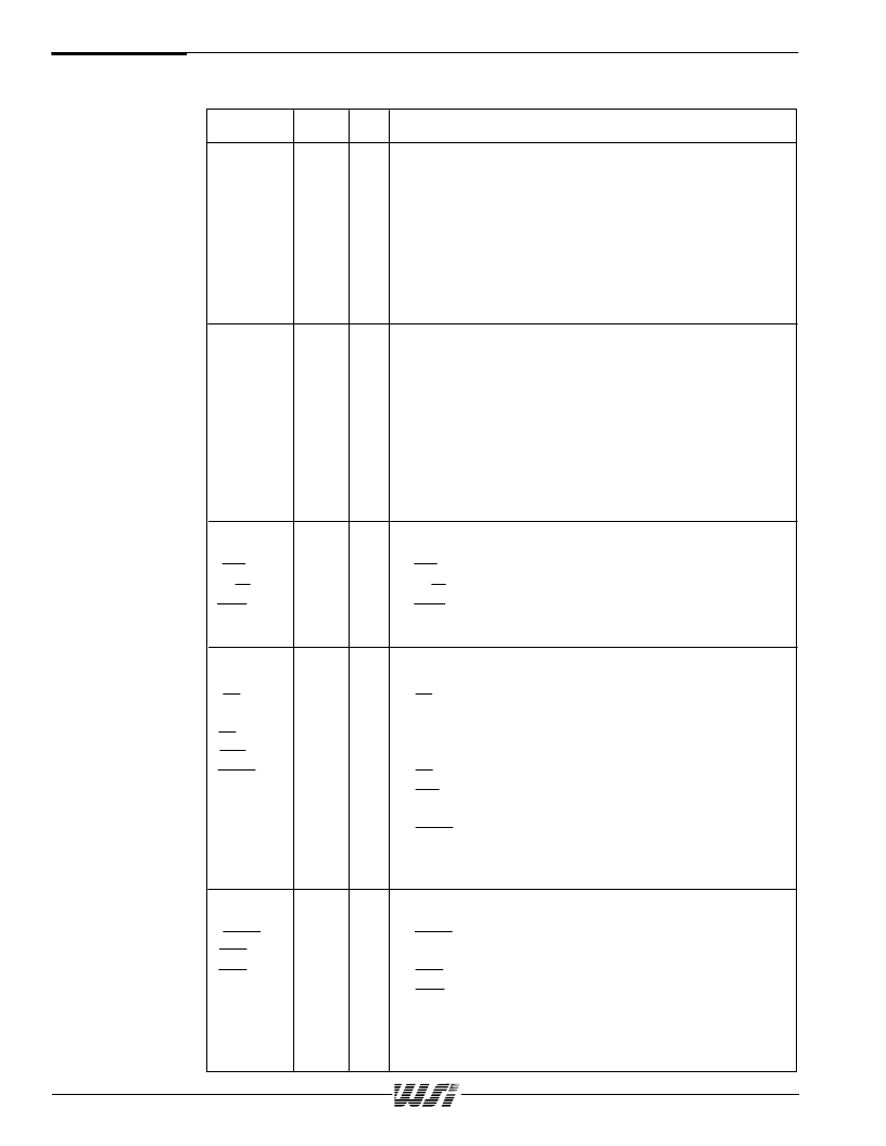
The following table describes the pin names and pin functions of the PSD6XXE1. Pins that
have multiple names and/or functions are defined by configuration.
Table 2.
PSD6XXE1 Pin
Descriptions
Pin Name
Pin
Type
Function Description
ADIO0–7
30–37
I/O
Address/Data Port, interface to Microcontroller Bus
1. Input pins for multiplexed low order address/data byte.
ALE or AS latches address A0-7. The PSD drives data
out only if read is active and one of the internal PSD
functional blocks is selected.
2. Address A0-7 inputs for non-multiplexed bus or 80C251
mode
3. A4/D0-A11/D7 inputs in 80C51XA mode
4. Address (or latched address) inputs to PLD
ADIO8–15
39–46
I/O
Address/Data Port, interface to Microcontroller Bus
1. Address A8-15 inputs in 8-bit data bus mode, or as
multiplexed high order address/data byte inputs in 16-bit
data bus mode. ALE or AS latches address A8-15.
The PSD drives data out only if read is active and one of
the internal PSD functional blocks is selected.
2. Address A8-15 inputs in non-multiplexed bus mode
3. AD8-AD15 inputs in 80C251 mode
4. A12-A19 or A12/D8 - A19/D15 inputs in 80C51XA mode
5. Address (or latched address) inputs to PLD
CNTL0)
47
I
Write Input pin with multiple configurations. Depending on
the MCU interface selected, this pin can be:
1. WR – active low write input
2. R_W – read/write pin, low for write bus cycle
3. WRL – for 16 bit data bus only, write to low byte, active low
4. Control signal (CNTL0) input to PLD
(WR,
R_W,
WRL)
CNTL1
50
I
Read or Data Strobe Input pin with multiple configurations.
Depending on the MCU interface selected, this pin can be:
1. RD – active low read input
2. E – E clock input.
During a write bus cycle, E is high and R/W is low
During a read bus cycle, E is high and R/W is high
3. DS – Data Strobe, active low
4. LDS – Strobe for low data byte, 16-bit data bus mode,
active low
5. PSEN – Program Select Enable, active low in read bus
cycle (80C251 configuration)
6. Control signal (CNTL1) input to PLD
(RD,
E,
DS,
LDS,
PSEN)
CNTL2
49
I
Read or other Control input pin with multiple configurations.
Depending on the MCU interface selected, this pin can be:
1. PSEN – Program Select enable, active low in code fetch
bus cycle
2. BHE – High byte enable, 16-bit data bus
3. UDS – Strobe for high data byte, 16-bit data bus mode,
active low
4. SIZ0 – Byte enable input
5. Control signal (CNTL2) input or general input to PLD
(PSEN,
BHE,
UDS,
SIZ0)
相关PDF资料 |
PDF描述 |
|---|---|
| PSD703S5 | Field Programmable Microcontroller Peripherals with Supervisory Functions(可编程逻辑,4K位SRAM,27个可编程I/O,通用PLD有66个输入) |
| PSD701S5 | Field Programmable Microcontroller Peripherals with Supervisory Functions(可编程逻辑,4K位SRAM,27个可编程I/O,通用PLD有66个输入) |
| PSD702S5 | Field Programmable Microcontroller Peripherals with Supervisory Functions(可编程逻辑,4K位SRAM,27个可编程I/O,通用PLD有66个输入) |
| PSD711S5 | Field Programmable Microcontroller Peripherals with Supervisory Functions(可编程逻辑,4K位SRAM,27个可编程I/O,通用PLD有66个输入) |
| PSD712S5 | Field Programmable Microcontroller Peripherals with Supervisory Functions(可编程逻辑,4K位SRAM,27个可编程I/O,通用PLD有66个输入) |
相关代理商/技术参数 |
参数描述 |
|---|---|
| PSD613E1-15L | 制造商:WSI 功能描述: |
| PSD613E1-70J | 制造商:WSI 功能描述: |
| PSD62 | 制造商:POWERSEM 制造商全称:POWERSEM 功能描述:Three Phase Rectifier Bridges |
| PSD6241212 | 制造商:TDK-Lambda Corporation 功能描述:DC/DC,DUAL-OUT,12/-12V,0.25/-0.25A,6W - Bulk |
| PSD6-24-1212 | 功能描述:DC/DC转换器 6W 12V 0.25A RoHS:否 制造商:Murata 产品: 输出功率: 输入电压范围:3.6 V to 5.5 V 输入电压(标称): 输出端数量:1 输出电压(通道 1):3.3 V 输出电流(通道 1):600 mA 输出电压(通道 2): 输出电流(通道 2): 安装风格:SMD/SMT 封装 / 箱体尺寸: |
发布紧急采购,3分钟左右您将得到回复。