- 您现在的位置:买卖IC网 > PDF目录368231 > PSD711S5 Field Programmable Microcontroller Peripherals with Supervisory Functions(可编程逻辑,4K位SRAM,27个可编程I/O,通用PLD有66个输入) PDF资料下载
参数资料
| 型号: | PSD711S5 |
| 英文描述: | Field Programmable Microcontroller Peripherals with Supervisory Functions(可编程逻辑,4K位SRAM,27个可编程I/O,通用PLD有66个输入) |
| 中文描述: | 现场可编程微控制器外围设备具有监督职能(可编程逻辑,4K的位的SRAM,27余个可编程输入/输出,通用PLD的有66个输入) |
| 文件页数: | 12/104页 |
| 文件大小: | 515K |
| 代理商: | PSD711S5 |
第1页第2页第3页第4页第5页第6页第7页第8页第9页第10页第11页当前第12页第13页第14页第15页第16页第17页第18页第19页第20页第21页第22页第23页第24页第25页第26页第27页第28页第29页第30页第31页第32页第33页第34页第35页第36页第37页第38页第39页第40页第41页第42页第43页第44页第45页第46页第47页第48页第49页第50页第51页第52页第53页第54页第55页第56页第57页第58页第59页第60页第61页第62页第63页第64页第65页第66页第67页第68页第69页第70页第71页第72页第73页第74页第75页第76页第77页第78页第79页第80页第81页第82页第83页第84页第85页第86页第87页第88页第89页第90页第91页第92页第93页第94页第95页第96页第97页第98页第99页第100页第101页第102页第103页第104页
PSD7XX Family
13-12
PSD7XX devices consist of several major functional blocks. Figure 1 shows the architecture
of the PSD7XX family. The functions of each block are described briefly in the following
sections. Many of the blocks perform multiple functions, and are user configurable.
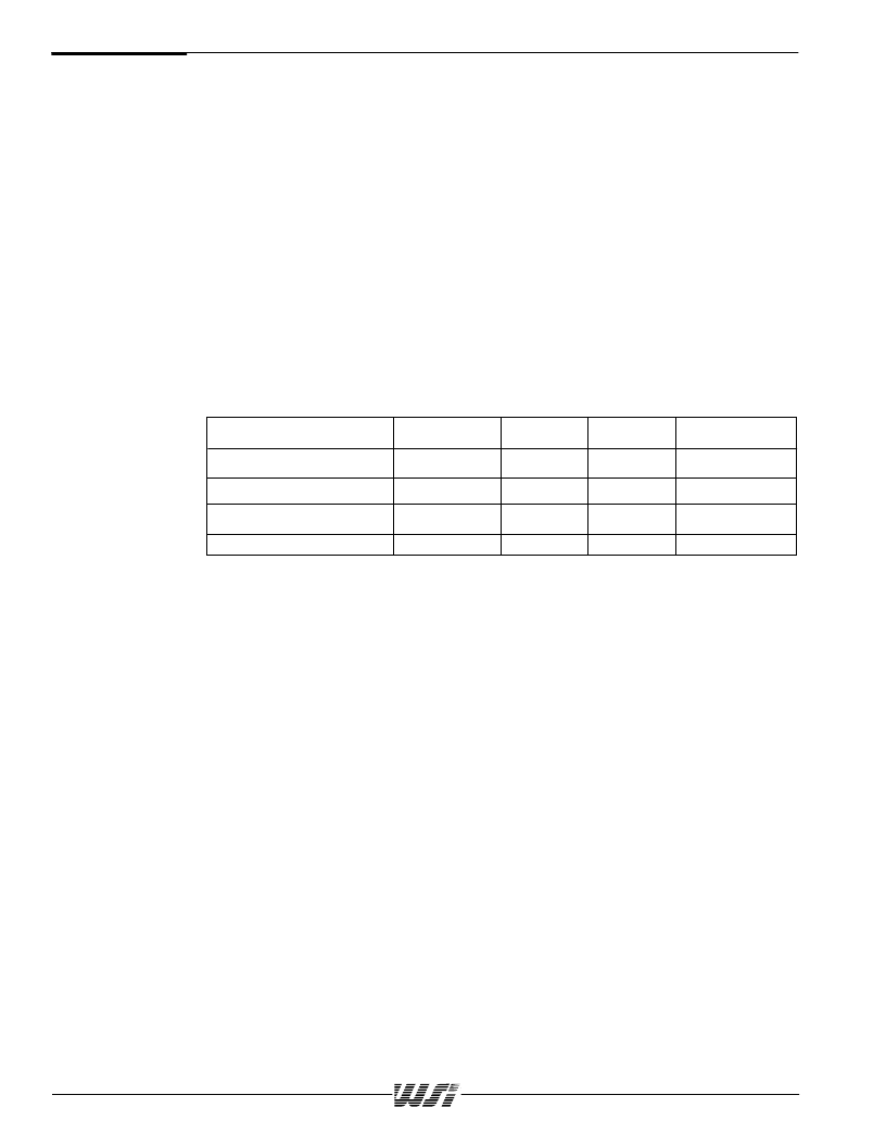
PLDs
The device contains four PLD blocks each optimized for a different function as shown in
Table 6. The functional partitioning of the PLDs reduces power consumption, optimizes
cost/performance and ease of design entry.
The Decode PLD (DPLD) is used to decode and generate chip selects for the PSD7XX
internal memory, registers and peripheral mode. The External Chip Select PLD (ECSPLD) is
optimized to generate chip selects for devices external to the PSD7XX. The General
Purpose PLD (GPLD) can implement user defined logic functions. The DPLD and ECSPLD
have combinatorial outputs while the GPLD has 12 Output Micro
Cells. The PSD7XX also
has 24 Input Micro
Cells that can be configured as inputs to the PLD. The PLDs receive
their inputs from the PLD Input bus and are differentiated by their output destinations,
number of product terms, and Micro
Cells.
The Peripheral PLD (PPLD) is dedicated to generate control signals for the WatchDog timer.
PSD7XX
Architectural
Overview
Name
Abbreviation
Inputs
Outputs
Product Terms
Decode PLD
DPLD
46
12
13
External Chip Select PLD
ECSPLD
24
7
7
General PLD
GPLD
66
12
110
Peripheral PLD
PPLD
66
2
2
Table 6.
I/O Ports
The PSD7XX has 27 I/O pins divided among four ports. Each I/O pin can be individually
configured to provide many functions. Ports A, B, C and D can be configured as standard
MCU I/O ports, PLD I/O, or latched address outputs for microcontrollers using multiplexed
address/data busses.
Ports A and B can also be configured as a data port for microcontrollers with a
non-multiplexed bus. In these modes, Port A is connected to D0–7 and Port B to D8–15.
Supervisory Functions
The PSD7XX provides all the supervisory functions required for an embedded system.
A voltage comparator monitors the system power supply and generates a reset if V
CC
drops
below internal or external reference voltages (hysterisis included). The polarity and duration
of the reset output signal is programmable.
A noise filter for the reset input is provided to debounce the source (pushbutton or other).
The internal PSD7XX SRAM is automatically switched to standby voltage if V
CC
drops
below the standby voltage value. When switchover occurs, the internal SRAM is write
protected and a single user defined chip select output immediately goes inactive. This
special chip select supports the use of an additional external battery backup SRAM (to
ensure low power consumption during a fault) or provides protection against inadvertent
writes to external FLASH or EEPROM.
A WatchDog timer is provided to monitor software integrity. Normal program flow will
continually reset the WatchDog timer. However, if program flow malfunctions and hangs up,
the timer will timeout and reset the system. This 9-bit WatchDog timer is programmable and
can supply its own independent clock source.
相关PDF资料 |
PDF描述 |
|---|---|
| PSD712S5 | Field Programmable Microcontroller Peripherals with Supervisory Functions(可编程逻辑,4K位SRAM,27个可编程I/O,通用PLD有66个输入) |
| PSD713S5 | Field Programmable Microcontroller Peripherals with Supervisory Functions(可编程逻辑,4K位SRAM,27个可编程I/O,通用PLD有66个输入) |
| PSD813F4 | Flash In System Programmable Mirocomputer Peripherals(闪速,在系统可编程微控制器外围器件,1M位闪速存储器,256K位EEPROM,16K位SRAM) |
| PSD813F | Flash In-System-Programmable Microcontroller Peripherals(闪速,在系统可编程微控制器外围器件,1M位闪速存储器,256K位EEPROM,16K位SRAM) |
| PSD813FH(中文) | Field Programmble Microcontroller Peripherals With Flash Memory(带闪存的现场可编程微控制器) |
相关代理商/技术参数 |
参数描述 |
|---|---|
| PSD711S5-15L | 制造商:WSI 功能描述: |
| PSD711S5-70L | 制造商:WSI 功能描述: |
| PSD712S5-15L | 制造商:WSI 功能描述: |
| PSD-7155 | 制造商:GAMEWELL-FCI 制造商全称:GAMEWELL-FCI 功能描述:Photoelectric smoke detector |
| PSD-7155D | 制造商:GAMEWELL-FCI 制造商全称:GAMEWELL-FCI 功能描述:Duct Housing, 4-wire, less detector head |
发布紧急采购,3分钟左右您将得到回复。