- 您现在的位置:买卖IC网 > PDF目录368232 > PSD835F1-70B81I (意法半导体) Single Ended Active Clamp/Reset PWM 16-SOIC -40 to 85 PDF资料下载
参数资料
| 型号: | PSD835F1-70B81I |
| 厂商: | 意法半导体 |
| 英文描述: | Single Ended Active Clamp/Reset PWM 16-SOIC -40 to 85 |
| 中文描述: | 在8片位微控制器可配置存储系统 |
| 文件页数: | 14/110页 |
| 文件大小: | 570K |
| 代理商: | PSD835F1-70B81I |
第1页第2页第3页第4页第5页第6页第7页第8页第9页第10页第11页第12页第13页当前第14页第15页第16页第17页第18页第19页第20页第21页第22页第23页第24页第25页第26页第27页第28页第29页第30页第31页第32页第33页第34页第35页第36页第37页第38页第39页第40页第41页第42页第43页第44页第45页第46页第47页第48页第49页第50页第51页第52页第53页第54页第55页第56页第57页第58页第59页第60页第61页第62页第63页第64页第65页第66页第67页第68页第69页第70页第71页第72页第73页第74页第75页第76页第77页第78页第79页第80页第81页第82页第83页第84页第85页第86页第87页第88页第89页第90页第91页第92页第93页第94页第95页第96页第97页第98页第99页第100页第101页第102页第103页第104页第105页第106页第107页第108页第109页第110页
PSD835G2
PSD8XX Family
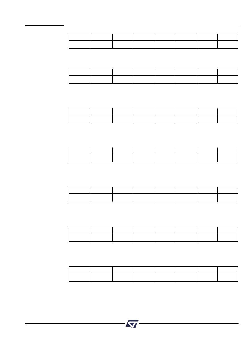
13
8.0
Register Bit
Definition
(cont.)
Bit 7
Bit 6
Bit 5
Bit 4
Bit 3
Bit 2
Bit 1
Bit 0
IMcell7
IMcell6
IMcell5
IMcell4
IMcell3
IMcell2
IMcell1
IMcell0
Input Micro
Cells – Ports A, B and C
Bit definitions: Read Only Registers
Read Input Micro
Cell[7:0] status on Ports A, B and C.
Bit 7
Bit 6
Bit 5
Bit 4
Bit 3
Bit 2
Bit 1
Bit 0
Mcella7
Mcella6
Mcella5
Mcella4
Mcella3
Mcella2
Mcella1
Mcella0
Output Micro
Cells A Register
Bit definitions:
Write Register:
Load Micro
CellA[7:0] with 0 or 1.
Read Register:
Read Micro
CellA[7:0] output status.
Output Micro
Cells B Register
Bit 7
Bit 6
Bit 5
Bit 4
Bit 3
Bit 2
Bit 1
Bit 0
Mcellb7
Mcellb6
Mcellb5
Mcellb4
Mcellb3
Mcellb2
Mcellb1
Mcellb0
Bit definitions:
Write Register:
Load Micro
CellB[7:0] with 0 or 1.
Read Register:
Read Micro
CellB[7:0] output status.
Mask Micro
Cells A Register
Bit 7
Bit 6
Bit 5
Bit 4
Bit 3
Bit 2
Bit 1
Bit 0
Mcella7
Mcella6
Mcella5
Mcella4
Mcella3
Mcella2
Mcella1
Mcella0
Bit definitions:
Register Bit <j> to 0 = allow Micro
CellA<j> flip flop to be loaded by MCU (default).
Register Bit <j> to 1 = does not allow Micro
CellA<j> flip flop to be loaded by MCU.
Bit 7
Bit 6
Bit 5
Bit 4
Bit 3
Bit 2
Bit 1
Bit 0
Mcellb7
Mcellb6
Mcellb5
Mcellb4
Mcellb3
Mcellb2
Mcellb1
Mcellb0
Mask Micro
Cells B Register
Bit definitions:
Register Bit <j> to 0 = allow Micro
CellB<j> flip flop to be loaded by MCU (default).
Register Bit <j> to 1 = does not allow Micro
CellB<j> flip flop to be loaded by MCU.
Bit 7
Bit 6
Bit 5
Bit 4
Bit 3
Bit 2
Bit 1
Bit 0
Sec7_Prot
Sec6_Prot
Sec5_Prot
Sec4_Prot
Sec3_Prot
Sec2_Prot
Sec1_Prot Sec0_Prot
Flash Protection Register
Bit definitions: Read Only Register
Sec<i>_Prot
1 = Flash Sector <i> is write protected.
Sec<i>_Prot
0 = Flash Sector <i> is not write protected.
Bit 7
Bit 6
Bit 5
Bit 4
Bit 3
Bit 2
Bit 1
Bit 0
Security_Bit
*
*
*
Sec3_Prot
Sec2_Prot
Sec1_Prot Sec0_Prot
Flash Boot Protection Register
Bit definitions:
Sec<i>_Prot
Sec<i>_Prot
1 = Boot Block Sector <i> is write protected.
0 = Boot Block Sector <i> is not write protected.
Security_Bit
0 = Security Bit in device has not been set.
1 = Security Bit in device has been set.
相关PDF资料 |
PDF描述 |
|---|---|
| PSD835F1-70J | Single Ended Active Clamp/Reset PWM 16-SOIC -40 to 85 |
| PSD835F1-70JI | Single Ended Active Clamp/Reset PWM 16-SOIC -40 to 85 |
| PSD835F1-70M | Single Ended Active Clamp/Reset PWM 16-SOIC -40 to 85 |
| PSD835F1-70MI | Single Ended Active Clamp/Reset PWM 16-PDIP -40 to 85 |
| PSD835F2-12U | Configurable Memory System on a Chip for 8-Bit Microcontrollers |
相关代理商/技术参数 |
参数描述 |
|---|---|
| PSD835G2-70U | 功能描述:静态随机存取存储器 5.0V 4M 70ns RoHS:否 制造商:Cypress Semiconductor 存储容量:16 Mbit 组织:1 M x 16 访问时间:55 ns 电源电压-最大:3.6 V 电源电压-最小:2.2 V 最大工作电流:22 uA 最大工作温度:+ 85 C 最小工作温度:- 40 C 安装风格:SMD/SMT 封装 / 箱体:TSOP-48 封装:Tray |
| PSD835G2-90U | 功能描述:静态随机存取存储器 5.0V 4M 90ns RoHS:否 制造商:Cypress Semiconductor 存储容量:16 Mbit 组织:1 M x 16 访问时间:55 ns 电源电压-最大:3.6 V 电源电压-最小:2.2 V 最大工作电流:22 uA 最大工作温度:+ 85 C 最小工作温度:- 40 C 安装风格:SMD/SMT 封装 / 箱体:TSOP-48 封装:Tray |
| PSD835G2-90UI | 功能描述:静态随机存取存储器 5.0V 4M 90ns RoHS:否 制造商:Cypress Semiconductor 存储容量:16 Mbit 组织:1 M x 16 访问时间:55 ns 电源电压-最大:3.6 V 电源电压-最小:2.2 V 最大工作电流:22 uA 最大工作温度:+ 85 C 最小工作温度:- 40 C 安装风格:SMD/SMT 封装 / 箱体:TSOP-48 封装:Tray |
| PSD835G2V-12UI | 功能描述:静态随机存取存储器 3.0V 4M 120ns RoHS:否 制造商:Cypress Semiconductor 存储容量:16 Mbit 组织:1 M x 16 访问时间:55 ns 电源电压-最大:3.6 V 电源电压-最小:2.2 V 最大工作电流:22 uA 最大工作温度:+ 85 C 最小工作温度:- 40 C 安装风格:SMD/SMT 封装 / 箱体:TSOP-48 封装:Tray |
| PSD835G2V-90U | 功能描述:静态随机存取存储器 3.0V 4M 90ns RoHS:否 制造商:Cypress Semiconductor 存储容量:16 Mbit 组织:1 M x 16 访问时间:55 ns 电源电压-最大:3.6 V 电源电压-最小:2.2 V 最大工作电流:22 uA 最大工作温度:+ 85 C 最小工作温度:- 40 C 安装风格:SMD/SMT 封装 / 箱体:TSOP-48 封装:Tray |
发布紧急采购,3分钟左右您将得到回复。