- 您现在的位置:买卖IC网 > PDF目录368236 > PSD835F1V-C-15JI (意法半导体) Configurable Memory System on a Chip for 8-Bit Microcontrollers PDF资料下载
参数资料
| 型号: | PSD835F1V-C-15JI |
| 厂商: | 意法半导体 |
| 英文描述: | Configurable Memory System on a Chip for 8-Bit Microcontrollers |
| 中文描述: | 在8片位微控制器可配置存储系统 |
| 文件页数: | 17/110页 |
| 文件大小: | 570K |
| 代理商: | PSD835F1V-C-15JI |
第1页第2页第3页第4页第5页第6页第7页第8页第9页第10页第11页第12页第13页第14页第15页第16页当前第17页第18页第19页第20页第21页第22页第23页第24页第25页第26页第27页第28页第29页第30页第31页第32页第33页第34页第35页第36页第37页第38页第39页第40页第41页第42页第43页第44页第45页第46页第47页第48页第49页第50页第51页第52页第53页第54页第55页第56页第57页第58页第59页第60页第61页第62页第63页第64页第65页第66页第67页第68页第69页第70页第71页第72页第73页第74页第75页第76页第77页第78页第79页第80页第81页第82页第83页第84页第85页第86页第87页第88页第89页第90页第91页第92页第93页第94页第95页第96页第97页第98页第99页第100页第101页第102页第103页第104页第105页第106页第107页第108页第109页第110页
PSD8XX Family
PSD835G2
16
9.0
The
PSD835G2
Functional
Blocks
As shown in Figure 1, the PSD835G2 consists of six major types of functional blocks:
J
Memory Blocks
J
PLD Blocks
J
Bus Interface
J
I/OPorts
J
Power Management Unit
J
JTAG-ISP Interface
The functions of each block are described in the following sections. Many of the blocks
perform multiple functions, and are user configurable.
9.1 Memory Blocks
The PSD835G2 has the following memory blocks:
The main Flash memory
Secondary Flash memory
SRAM.
The memory select signals for these blocks originate from the Decode PLD (DPLD) and
are user-defined in PSDsoft.
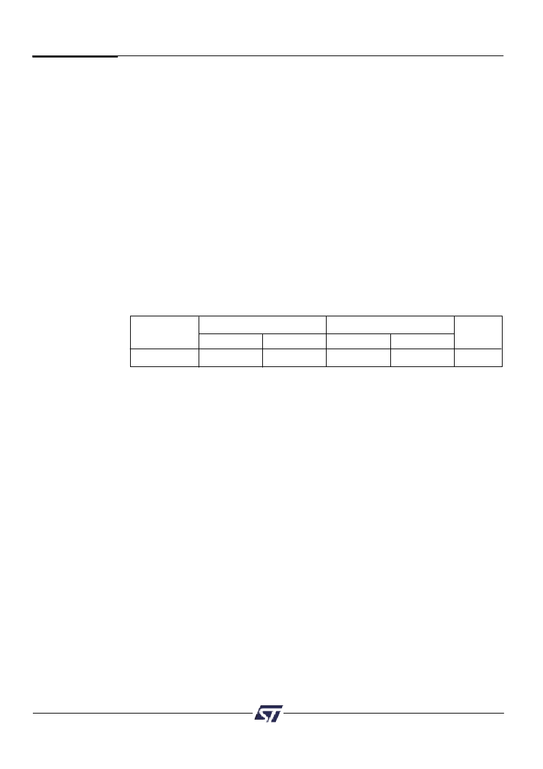
Table 7 summarizes which versions of the PSD835G2 contain which memory blocks.
Main Flash
Secondary Flash
Block Size
Device
Flash Size
Sector Size
Sector Size
SRAM
PSD835G2
512KB
64KB
32KB
8KB
8KB
Table 7. Memory Blocks
9.1.1 Main Flash and Secondary Flash Memory Description
The main Flash memory block is divided evenly into eight sectors. The secondary Flash
memory is divided into four sectors of eight Kbytes each. Each sector of either memory
can be separately protected from program and erase operations.
Flash memory may be erased on a sector-by-sector basis and programmed word-by-word.
Flash sector erasure may be suspended while data is read from other sectors of memory
and then resumed after reading.
During a program or erase of Flash, the status can be output on the Rdy/Bsy pin of Port
PE4. This pin is set up using PSDsoft.
9.1.1.1 Memory Block Selects
The decode PLD in the PSD835G2 generates the chip selects for all the internal memory
blocks (refer to the PLD section). Each of the eight Flash memory sectors have a
Flash Select signal (FS0-FS7) which can contain up to three product terms. Each of the
four Secondary Flash memory sectors have a Select signal (CSBOOT0-3) which can
contain up to three product terms. Having three product terms for each sector select signal
allows a given sector to be mapped in different areas of system memory. When using a
microcontroller (80C51) with separate Program and Data space, these flexible select
signals allow dynamic re-mapping of sectors from one space to the other before and after
IAP.
相关PDF资料 |
PDF描述 |
|---|---|
| PSD835F1V-C-15M | Configurable Memory System on a Chip for 8-Bit Microcontrollers |
| PSD835F1V-C-15MI | Configurable Memory System on a Chip for 8-Bit Microcontrollers |
| PSD835F1V-C-15U | Configurable Memory System on a Chip for 8-Bit Microcontrollers |
| PSD835F1V-C-15UI | Configurable Memory System on a Chip for 8-Bit Microcontrollers |
| PSD835F1V-C-20B81 | Configurable Memory System on a Chip for 8-Bit Microcontrollers |
相关代理商/技术参数 |
参数描述 |
|---|---|
| PSD835G2-70U | 功能描述:静态随机存取存储器 5.0V 4M 70ns RoHS:否 制造商:Cypress Semiconductor 存储容量:16 Mbit 组织:1 M x 16 访问时间:55 ns 电源电压-最大:3.6 V 电源电压-最小:2.2 V 最大工作电流:22 uA 最大工作温度:+ 85 C 最小工作温度:- 40 C 安装风格:SMD/SMT 封装 / 箱体:TSOP-48 封装:Tray |
| PSD835G2-90U | 功能描述:静态随机存取存储器 5.0V 4M 90ns RoHS:否 制造商:Cypress Semiconductor 存储容量:16 Mbit 组织:1 M x 16 访问时间:55 ns 电源电压-最大:3.6 V 电源电压-最小:2.2 V 最大工作电流:22 uA 最大工作温度:+ 85 C 最小工作温度:- 40 C 安装风格:SMD/SMT 封装 / 箱体:TSOP-48 封装:Tray |
| PSD835G2-90UI | 功能描述:静态随机存取存储器 5.0V 4M 90ns RoHS:否 制造商:Cypress Semiconductor 存储容量:16 Mbit 组织:1 M x 16 访问时间:55 ns 电源电压-最大:3.6 V 电源电压-最小:2.2 V 最大工作电流:22 uA 最大工作温度:+ 85 C 最小工作温度:- 40 C 安装风格:SMD/SMT 封装 / 箱体:TSOP-48 封装:Tray |
| PSD835G2V-12UI | 功能描述:静态随机存取存储器 3.0V 4M 120ns RoHS:否 制造商:Cypress Semiconductor 存储容量:16 Mbit 组织:1 M x 16 访问时间:55 ns 电源电压-最大:3.6 V 电源电压-最小:2.2 V 最大工作电流:22 uA 最大工作温度:+ 85 C 最小工作温度:- 40 C 安装风格:SMD/SMT 封装 / 箱体:TSOP-48 封装:Tray |
| PSD835G2V-90U | 功能描述:静态随机存取存储器 3.0V 4M 90ns RoHS:否 制造商:Cypress Semiconductor 存储容量:16 Mbit 组织:1 M x 16 访问时间:55 ns 电源电压-最大:3.6 V 电源电压-最小:2.2 V 最大工作电流:22 uA 最大工作温度:+ 85 C 最小工作温度:- 40 C 安装风格:SMD/SMT 封装 / 箱体:TSOP-48 封装:Tray |
发布紧急采购,3分钟左右您将得到回复。